TC1796
System Units (Vol. 1 of 2)
Clock System and Control
User’s Manual 3-3 V2.0, 2007-07
Clock, V2.0
3.2 Clock Generation Unit
The PLL can convert a low-frequency external clock signal to a high-speed internal clock
for maximum performance. The PLL also has fail-safe logic that detects degenerate
external clock behavior such as abnormal frequency deviations or a total loss of the
external clock. It can execute emergency actions if it loses its lock on the external clock.
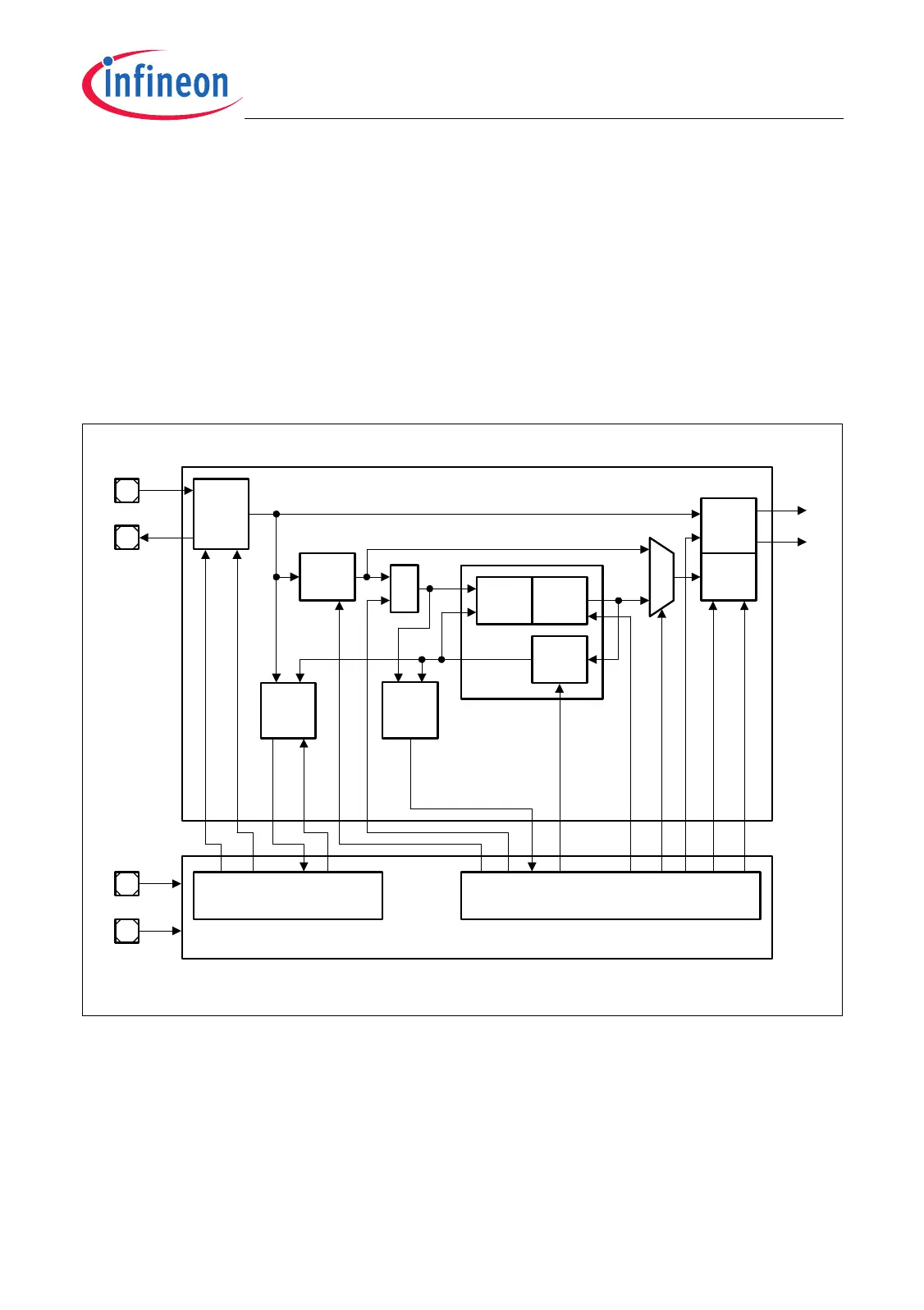
The Clock Generation Unit (CGU) in the TC1796, shown in Figure 3-2, consists
basically of an oscillator circuit and a Phase-Locked Loop (PLL). The operation of the
CGU is controlled by two registers, OSC_CON and PLL_CLC, which are located in the
System Control Unit (SCU).
Figure 3-2 CGU Detailed Block Diagram
MCB05600
Phase
Detect.
VCO
N-
Divider
PLL
KDIV
BYPASS
P5.3 /
TXD1A
Main
Osc.
Circuit
XTAL1
XTAL2
Osc.
Run
Detect.
f
VCO
f
N
≥1 f
P
M
U
X
P-
Divider
PLL
Lock
Detect.
Clock
Output
Control
f
OSC
K-
Divider
f
CPU
f
SYS
Clock Generation Unit (CGU)
VCOSEL
VCOBYP
SYSFS
BYPPIN
NDIV
LOCK
OSCDSIC
PDIV
OSCR
OGC
MOSC
Oscillator Control Register
OSC_CON
PLL Clock Control and Status Register
PLL_CLC
ORDRES
System Control Unit (SCU)

 Loading...