TC1796
System Units (Vol. 1 of 2)
CPU Subsystem
User’s Manual 2-50 V2.0, 2007-07
CPU, V2.0
For JLI, JEQ.A, JNE.A JNZ.A, JZ.A Instructions:
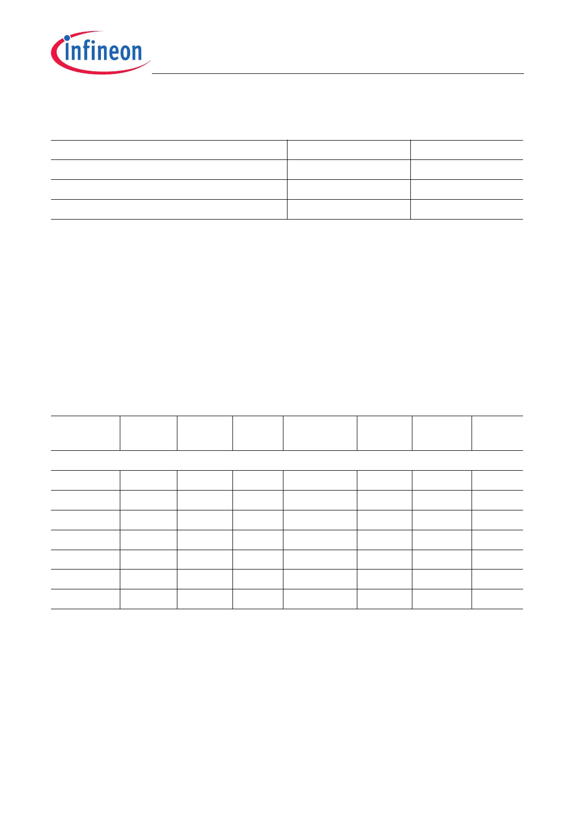
2.7.2.3 Load Instruction Timing
Load instructions can produce two results if they use the pre-increment, post-increment,
circular or bit-reverse addressing modes. Hence, in those cases there are two latencies
that must be specified, the result latency for the value loaded from memory and the
address latency for using the updated address register result.
• Each instruction is single issued.
• The memory references is naturally aligned.
• The memory accessed takes a single cycle to return a data item.
• Timing is best case; no cache misses, no pending stores.
Flow Latency Repeat Rate
Correctly predicted, not taken 1 1
Correctly predicted, taken 2 2
Wrongly predicted 3 2
Table 2-16 Load Instruction Timing
Instruction Addr.
Latency
Result
Latency
Repeat
Rate
Instruction Addr.
Latency
Result
Latency
Repeat
Rate
Load Instructions
LD.A 121LD.Q 11 1
LD.B 111LD.W 11 1
LD.BU 111LDLCX 44 4
LD.D 111LDUCX 44 4
LD.DA 121SWAP.W 22 2
LD.H 111LEA
1)
1) The addressing mode returning an updated address is not relevant for this instruction.
–1 1
LD.HU 111

 Loading...