TC1796
System Units (Vol. 1 of 2)
Clock System and Control
User’s Manual 3-16 V2.0, 2007-07
Clock, V2.0
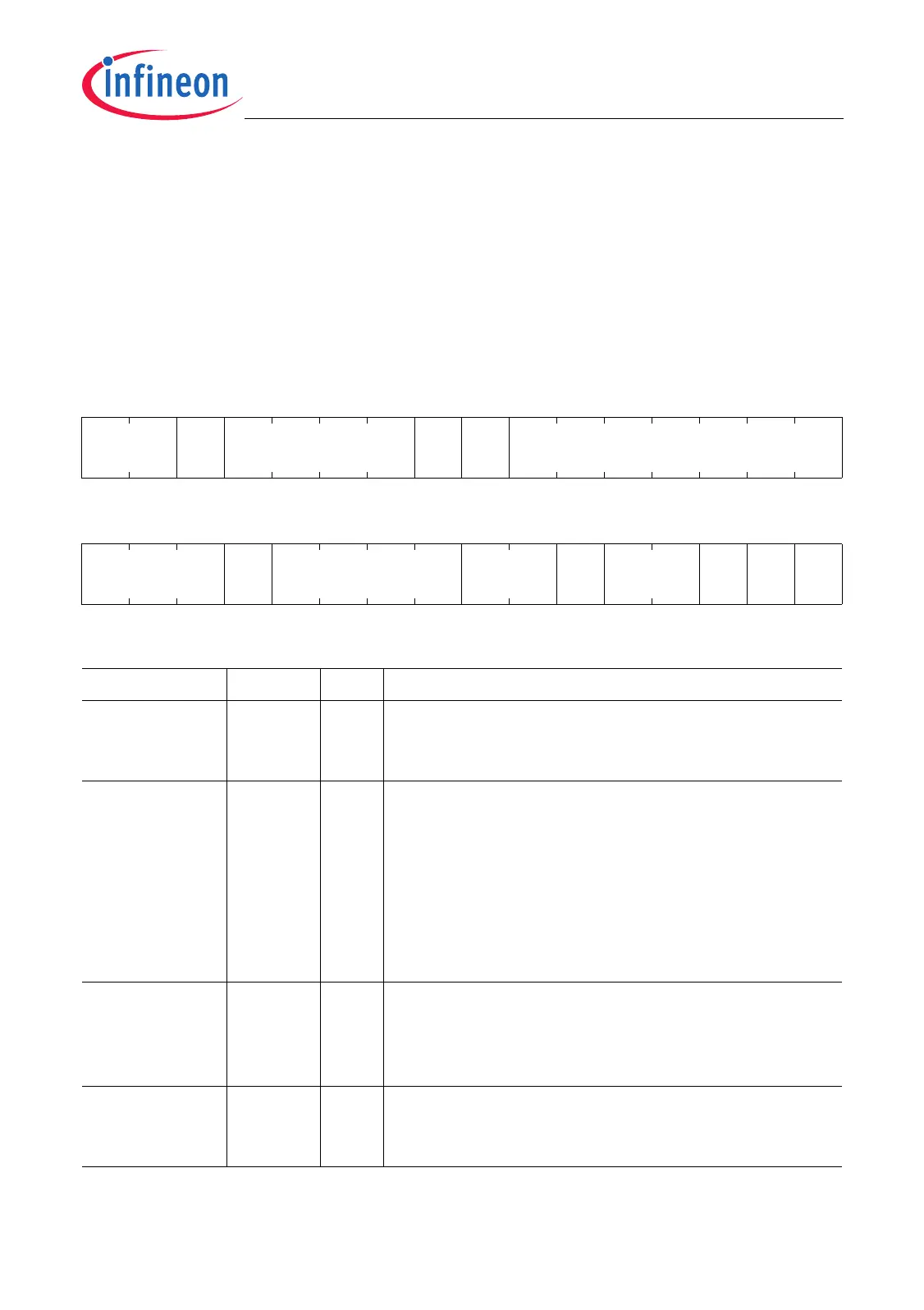
3.2.2.3 PLL Clock Control and Status Register
The PLL Clock Control and Status Register PLL_CLC is located in the address range of
the System Control Unit (see Page 5-62). It holds the hardware configuration bits of the
PLL and provides the control for the N, P and K-Dividers as well as the PLL lock status
bit. Register PLL_CLC is Endinit-protected.
PLL_CLC
PLL Clock Control Register (F0000040
H
) Reset Values: see Table 3-6
31 30 29 28 27 26 25 24 23 22 21 20 19 18 17 16
0
BYP
PIN
0
OSC
DISC
0NDIV
r rh r rwh r rw
1514131211109876543210
PDIV 0 KDIV VCOSEL
VCO
BYP
0
SYS
FS
RES
LD
LO
CK
rw r rw rw rw r rw rwh rh
Field Bits Type Description
LOCK 0rhPLL Lock Status Flag
0
B
PLL is not locked (default after reset)
1
B
PLL is locked
RESLD 1rwhRestart Lock Detection
Writing a 1 to this bit will clear the LOCK flag and
restart the PLL lock detection. After written with a 1,
this bit is reset automatically to 0 and therefore
always read back as 0. This bit becomes activated
with a power-on reset operation.
0
B
No operation
1
B
PLL lock detection is restarted.
SYSFS 2rwSystem Frequency Select
Selects the f
CPU
-to-f
SYS
clock ratio.
0
B
Ratio f
CPU
/f
SYS
is 2/1 (default after reset).
1
B
The ratio f
CPU
/f
SYS
is 1/1.
VCOBYP 5rwVCO Bypass Mode Selection
0
B
Normal operation (default after reset)
1
B
VCO Bypass Mode selected

 Loading...