TC1796
System Units (Vol. 1 of 2)
Direct Memory Access Controller
User’s Manual 12-105 V2.0, 2007-07
DMA, V2.0
12.3.3.1 Clock Control Register
The Clock Control Register controls the f
DMA
module clock signal. This clock is also used
for the MLI modules as a common clock that can be individually divided for the MLI
modules.
Note: After a hardware reset operation, the DMA module is enabled.
Note: The Suspend Mode does not modify any of the registers.
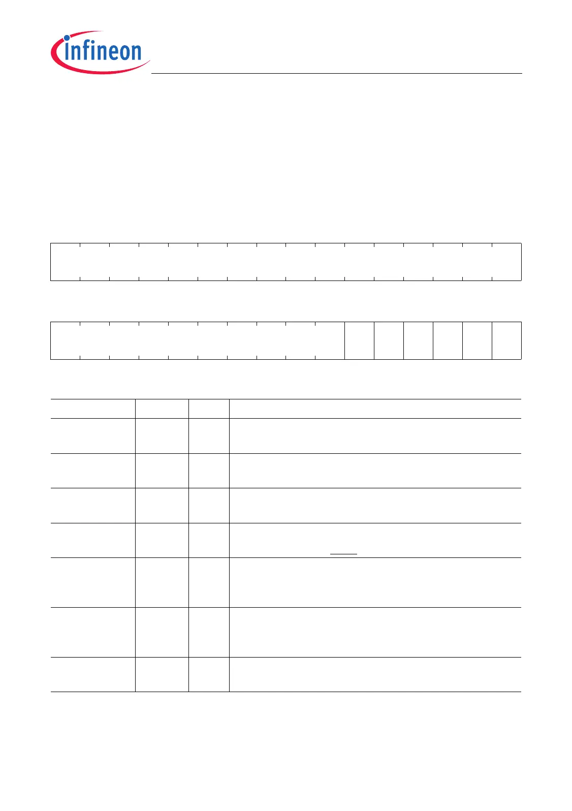
DMA_CLC
DMA Clock Control Register (000
H
) Reset Value: 0000 0000
H
31 30 29 28 27 26 25 24 23 22 21 20 19 18 17 16
0
r
1514131211109876543210
0
FS
OE
SB
WE
0
SP
EN
DISS DISR
r rwwrwrw r rw
Field Bits Type Description
DISR 0rwModule Disable Request Bit
Used for enable/disable control of the module
DISS 1rModule Disable Status Bit
Bit indicates the current status of the module
SPEN 2rwModule Suspend Enable for OCDS
Used to enable the suspend mode.
0 3rwReserved;
Returns 0 if read; must be written with 0.
SBWE 4wModule Suspend Bit Write Enable for OCDS
Determines whether SPEN and FSOE are write-
protected.
FSOE 5rwFast Switch Off Enable
Used for fast clock switch off in OCSD Suspend
Mode.
0 [31:6] r Reserved
Read as 0; should be written with 0.

 Loading...