TC1796
Peripheral Units (Vol. 2 of 2)
Analog-to-Digital Converter (ADC)
User’s Manual 25-105 V2.0, 2007-07
ADC, V2.0
25.3.3.1 ADC Clock Control Register
The clock control register makes it possible to control (enable/disable) the clock signal
f
CLC
under certain conditions. Both ADCs are controlled by one common clock control
register ADC0_CLC. After a reset operation, the ADC0 and ADC1 modules are disabled
and the module clock signals f
CLC
and f
ADC
are switched off.
Note: Additional details on the clock control register functionality are described in section
“Clock Control Register CLC” on Page 3-24 of the TC1796 User’s Manual
System Units part (Volume 1).
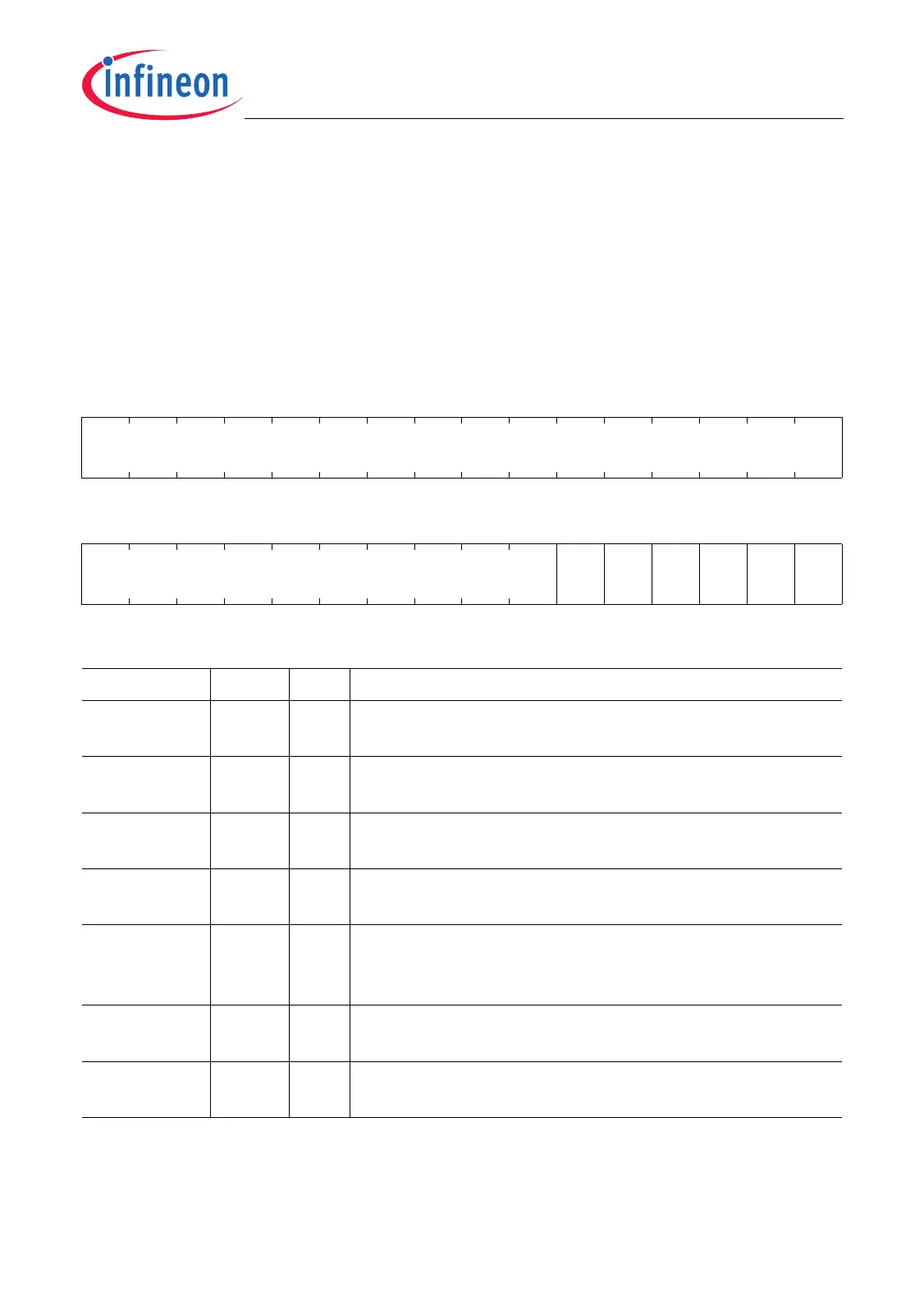
ADC0_CLC
ADC Clock Control Register (000
H
) Reset Value: 0000 0003
H
31 30 29 28 27 26 25 24 23 22 21 20 19 18 17 16
0
r
1514131211109876543210
0
FS
OE
SB
WE
E
DIS
SP
EN
DIS
S
DIS
R
r rwwrwrw r rw
Field Bits Type Description
DISR 0rwModule Disable Request Bit
Used for enable/disable control of the module.
DISS 1rModule Disable Status Bit
Bit indicates the current status of the module.
SPEN 2rwModule Suspend Enable for OCDS
Used to enable the suspend mode.
EDIS 3rwExternal Request Disable
Used to control the external clock disable request.
SBWE 4wModule Suspend Bit Write Enable for OCDS
Determines whether SPEN and FSOE are write-
protected.
FSOE 5rwFast Switch Off Enable
Used for fast clock switch off in suspend mode.
0 [31:6] r Reserved
Read as 0; should be written with 0.

 Loading...