TC1796
System Units (Vol. 1 of 2)
Program Memory Unit
User’s Manual 7-61 V2.0, 2007-07
PMU, V2.0
7.3 Emulation Interface
The emulation memory interface shown in Figure 7-1 is always disabled in the TC1796
device. This interface is a 64-bit wide memory interface that controls an emulation
memory in the TC1796 emulation device, called TC1796ED. Segment 8 and 10 reserves
512 Kbyte for the emulation memory interface.
In the TC1796, a CPU read access from the emulation memory region causes a DSE
trap, a PLMB and a DLMB bus error. If the emulation memory region read access is
initiated by a SPB master (e.g. PCP or DMA), additionally a SPB error is generated.
Write accesses to the emulation memory region by any master causes a PLMB bus
error.
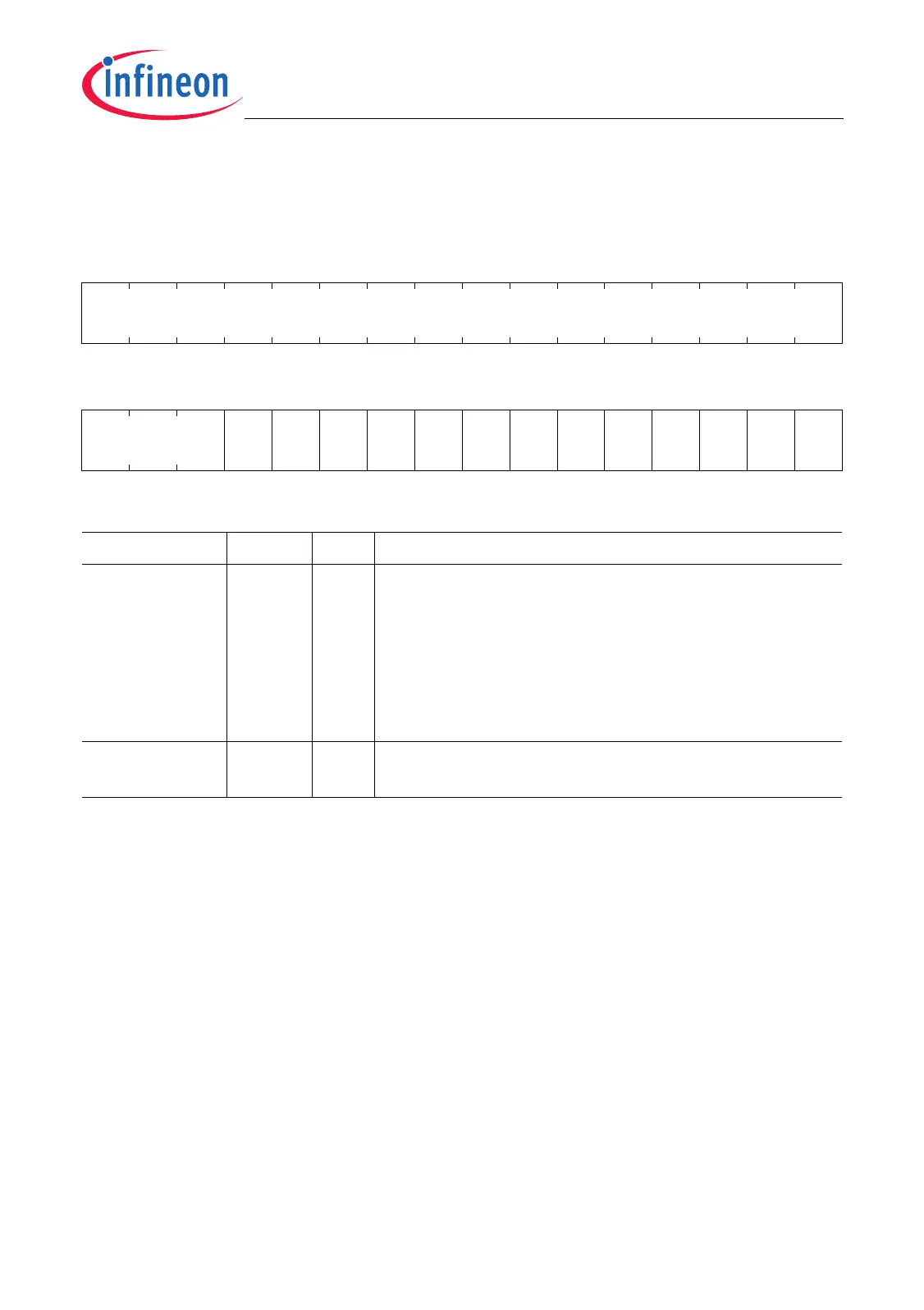
FLASH_PROCON2
Flash Protection Configuration Register User 2
(1028
H
) Reset Value: 0000 XXXX
H
31 30 29 28 27 26 25 24 23 22 21 20 19 18 17 16
0
r
1514131211109876543210
0 S12L S11L S10L S9L S8L S7L S6L S5L S4L S3L S2L S1L S0L
r rhrhrhrhrhrhrhrhrhrhrhrhrh
Field Bits Type Description
SnL
(n = 0-12)
nrhSector with OTP Protection (User 2)
These bits indicate whether OTP protection is
installed and locked for sector n.
0
B
No OTP protection installed for sector n.
1
B
OTP protection installed for sector n.
Reprogramming of this sector is no longer
possible.
0 [31:13] r Reserved
Read as 0.
 Loading...