TC1796
Peripheral Units (Vol. 2 of 2)
Analog-to-Digital Converter (ADC)
User’s Manual 25-109 V2.0, 2007-07
ADC, V2.0
25.3.4.1 Input/Output Control Register
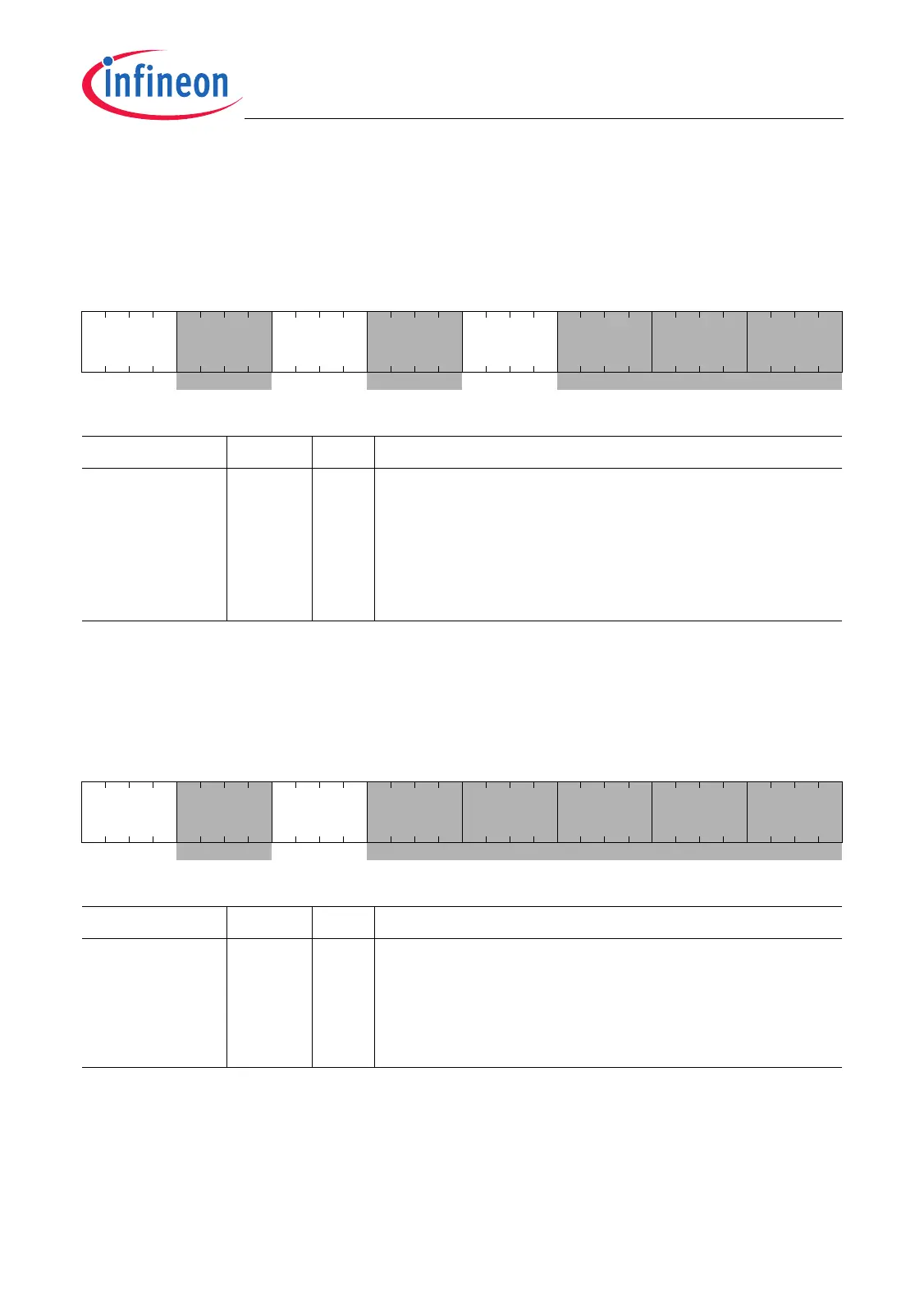
P7_IOCR0
Port 7 Input/Output Control Register 0 (10
H
) Reset Value: 2020 2020
H
31 28 23 20 15 12 7 4 0
PC3 0PC20PC10 PC0 0
rw rrwrrwr rw r
Field Bits Type Description
PC1,
PC2,
PC3
[15:12],
[23:20],
[31:28]
rw Port Output Control for Port 7 Pins 0-3
1)
These bit fields determine the output port
functionality:
Port input/output control for P7.1/AD0EMUX2
Port input/output control for P7.2/AD0EMUX0
Port input/output control for P7.3/AD0EMUX1
1) Coding of bit field see Table 25-15. Shaded bits and bit fields are “don’t care” for ADC I/O port control.
P7_IOCR4
Port 7 Input/Output Control Register 4 (14
H
) Reset Value: 2020 2020
H
31 28 23 20 15 12 7 4 0
PC7 0PC60 PC5 0 PC4 0
rw rrwr rw r rw r
Field Bits Type Description
PC6,
PC7
[23:20],
[31:28]
rw Port Output Control for Port 7 Pins 4-7
1)
These bit fields determine the output port
functionality:
Port input/output control for P7.6/AD1EMUX0
Port input/output control for P7.7/AD1EMUX1
1) Coding of bit field see Table 25-15. Shaded bits and bit fields are “don’t care” for ADC I/O port control.

 Loading...