TC1796
System Units (Vol. 1 of 2)
Register Overview
User’s Manual 18-2 V2.0, 2007-07
Regs, V2.0
18.1 Address Map of Segment 15
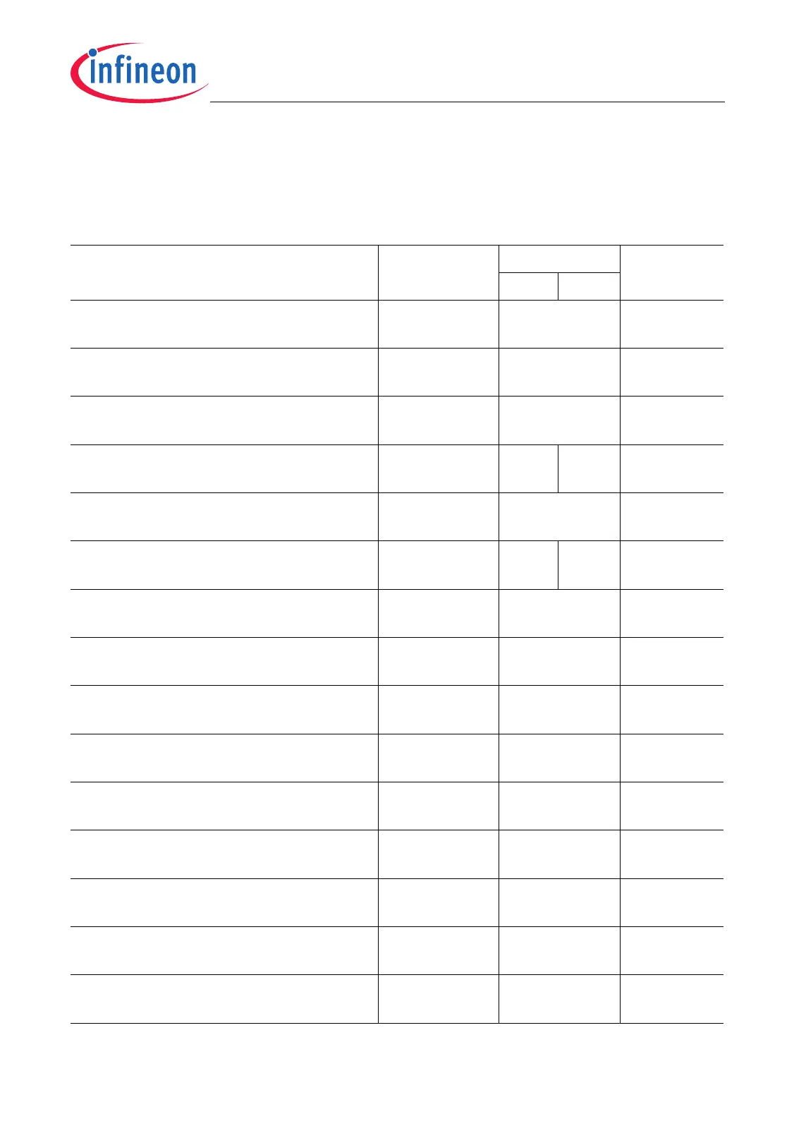
Table 18-2 shows the block address map of Segment 15.
Table 18-2 Block Address Map of Segment 15
Unit Address
Range
Access Mode Size
Read Write
System Control Unit (SCU) and
Watchdog Timer (WDT)
F000 0000
H
-
F000 00FF
H
see
Page 18-7
256 byte
System Peripheral Bus Control Unit
(SBCU)
F000 0100
H
-
F000 01FF
H
see
Page 18-11
256 byte
System Timer (STM) F000 0200
H
-
F000 02FF
H
see
Page 18-13
256 byte
Reserved F000 0300
H
-
F000 03FF
H
BE BE –
On-Chip Debug Support (Cerberus) F000 0400
H
-
F000 04FF
H
see
Page 18-14
256 byte
Reserved F000 0500
H
-
F000 07FF
H
BE BE –
MicroSecond Channel 0 (MSC0) F000 0800
H
-
F000 08FF
H
see
Page 18-16
256 byte
MicroSecond Channel 1 (MSC1) F000 0900
H
-
F000 09FF
H
see
Page 18-17
256 byte
Async./Sync. Serial Interface 0 (ASC0) F000 0A00
H
-
F000 0AFF
H
see
Page 18-20
256 byte
Async./Sync. Serial Interface 1 (ASC1) F000 0B00
H
-
F000 0BFF
H
see
Page 18-21
256 byte
Port 0 F000 0C00
H
-
F000 0CFF
H
see
Page 18-22
256 byte
Port 1 F000 0D00
H
-
F000 0DFF
H
see
Page 18-23
256 byte
Port 2 F000 0E00
H
-
F000 0EFF
H
see
Page 18-24
256 byte
Port 3 F000 0F00
H
-
F000 0FFF
H
see
Page 18-25
256 byte
Port 4 F000 1000
H
-
F000 10FF
H
see
Page 18-26
256 byte

 Loading...