TC1796
Peripheral Units (Vol. 2 of 2)
General Purpose Timer Array (GPTA)
User’s Manual 24-150 V2.0, 2007-07
GPTA, V2.0
24.3 GPTA0/1 Kernel Registers
This section describes the kernel registers of the GPTA0 module. The complete and
detailed address maps of the GPTA0, GPTA1, and LTCA2 modules is described in
Table 18-20 on Table 18-20, in Table 18-21 on Table 18-21, and in Table 18-22 on
Table 18-22 of the TC1796 User’s Manual System Units part (Volume 1).
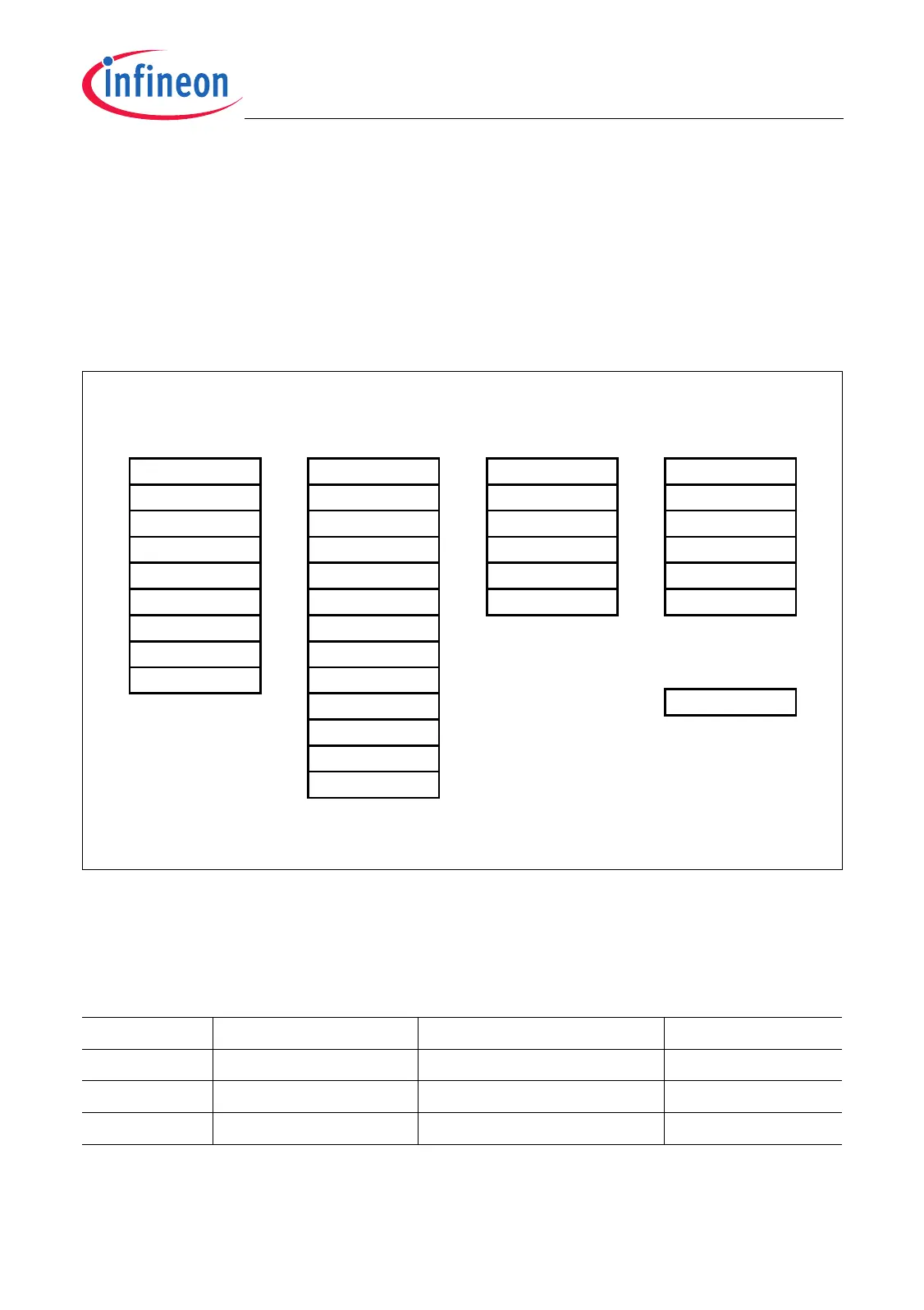
GPTA Kernel Register Overview
Figure 24-73 GPTA0 and GPTA1 Kernel Registers
In the TC1796, the registers of the GPTA modules are located in the following address
ranges.
Table 24-16 Registers Address Space
Module Base Address End Address Note
GPTA0 F000 1800
H
F000 1FFF
H
–
GPTA1 F000 2000
H
F000 27FF
H
–
LTCA2 F000 2800
H
F000 2FFF
H
–
1) k = 0-5
2) k = 0-3
3) k = 0-2
4) k = 00 - 31
5) k = 00 - 63
6) n = 0- 3
7) g = 0- 13
8) g = 0- 7
9) g = 0- 3
MCA05982_mod
FPCTIMk
Control Registers Interrupt & IOLS
Registers
Data Registers
DCMTIMk
DCMCAVk
SRSCn
DCMCOVk
PLLMTI
PLLSTP
PLLCNT
PLLREV
PLLDTR
GTTIMk
GTREVk
GTCXRk
LTCXRk
SRSSn
FPCSTAT
FPCCTRk
PDLCTR
DCMCTRk
PLLCTR
CKBCTR
GTCTRk
GTCCTRk
LTCCTRk
SRNR
MRACTL
MRADIN
MRADOUT
1)
2)
2)
2)
2)
1) 6)
3)
3)
4)
4)
5)
5)
6)
3)
Multiplexer Array
FIFO Registers
OMRCLg
OMRCHg
LIMCRLg
LIMCRHg
GIMCRLg
GIMCRHg
7)
7)
9)
9)
8)
8)
Note : The Multiplexer Array FIFO registers are not directly accessible !
ID
Identification
Register

 Loading...