TC1796
Peripheral Units (Vol. 2 of 2)
General Purpose Timer Array (GPTA)
User’s Manual 24-170 V2.0, 2007-07
GPTA, V2.0
24.3.6 Global Timer Registers
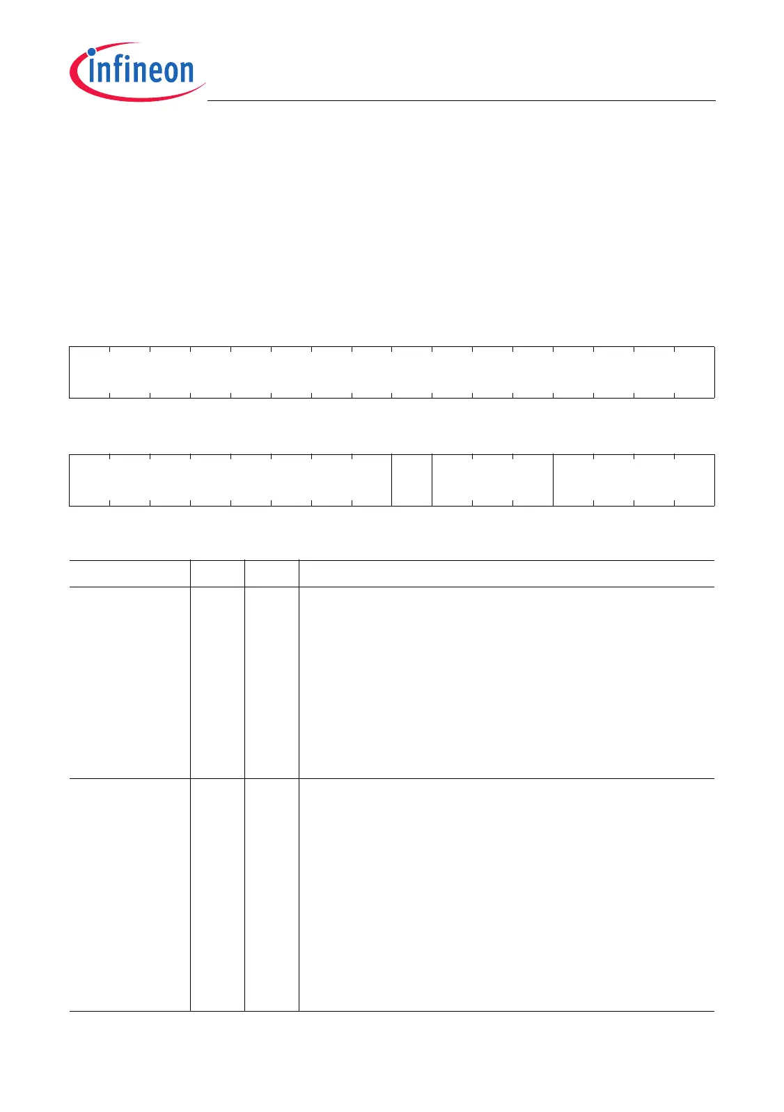
GPTA0_GTCTRk (k = 0-1)
GPTA0 Global Timer Control Register k
(0E0
H
+k*10
H
) Reset Value: 0000 0000
H
GPTA1_GTCTRk (k = 0-1)
GPTA1 Global Timer Control Register k
(0E0
H
+k*10
H
) Reset Value: 0000 0000
H
31 30 29 28 27 26 25 24 23 22 21 20 19 18 17 16
0
r
1514131211109876543210
0RENMUXSCO
rrwrwrw
Field Bits Type Description
SCO [3:0] rw TGE Flag Source Selection
This bit field determines the bit of the operation result
“GTk timer value - data bus value” which is used as
TGE flag.
0000
B
10
th
bit is used as TGE flag.
0001
B
11
th
bit is used as TGE flag.
…
B
…
1110
B
24
th
bit is used as TGE flag.
1111
B
25
th
bit is used as TGE flag.
MUX [6:4] rw Timer Clock Selection
One of eight available clock bus lines is selected as the
timer GTk clock.
000
B
Clock bus line CLK0 selected
001
B
Clock bus line CLK1 selected
010
B
Clock bus line CLK2 selected
011
B
Clock bus line CLK3 selected
100
B
Clock bus line CLK4 selected
101
B
Clock bus line CLK5 selected
110
B
Clock bus line CLK6 selected
111
B
Clock bus line CLK7 selected

 Loading...