TC1796
System Units (Vol. 1 of 2)
General Purpose I/O Ports and Peripheral I/O Lines
User’s Manual 10-2 V2.0, 2007-07
Ports, V2.0
10.1 Basic Port Operation
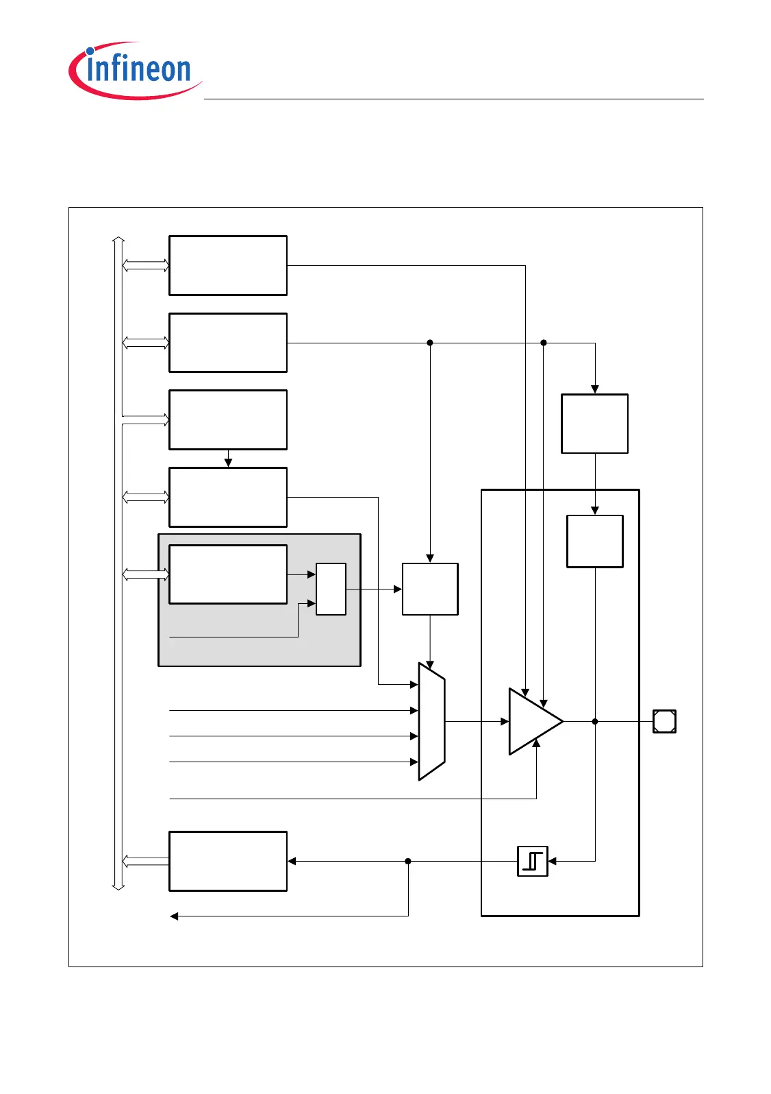
Figure 10-2 is a general block diagram of a TC1796 GPIO port line.
Figure 10-2 General Structure of a Port Pin
MCA05653
Pull-up
Pull-down
Control
ALT1
MUX
Select
Pin
Schmitt
Trigger
AltDataIn
System Peripheral Bus (SPB)
Pn_OMR
Output
Modification Reg.
Pn_ESR
Emergency Stop
Register
Pn_IOCR
Input/Output
Control Register
Pn_OUT
Data Output
Register
ALT2
ALT3
&
EMSTOP
MUX
Control
TC[1:0]
Pn_IN
Data Input
Register
Output
Driver
Pad Control Logic
Pull
Devices
Only available for GPTA lines
Pn_PDRx
Pad Driver
Mode Registers

 Loading...