TC1796
Peripheral Units (Vol. 2 of 2)
Analog-to-Digital Converter (ADC)
User’s Manual 25-57 V2.0, 2007-07
ADC, V2.0
25.2 ADC0/ADC1 Kernel Registers
This section describes the kernel registers of the ADC module. All ADC kernel register
names described in this section will be referenced in other parts of the TC1796 User’s
Manual by the module name prefix “ADC0_” for the ADC0 interface and “ADC1_” for the
ADC1 module.
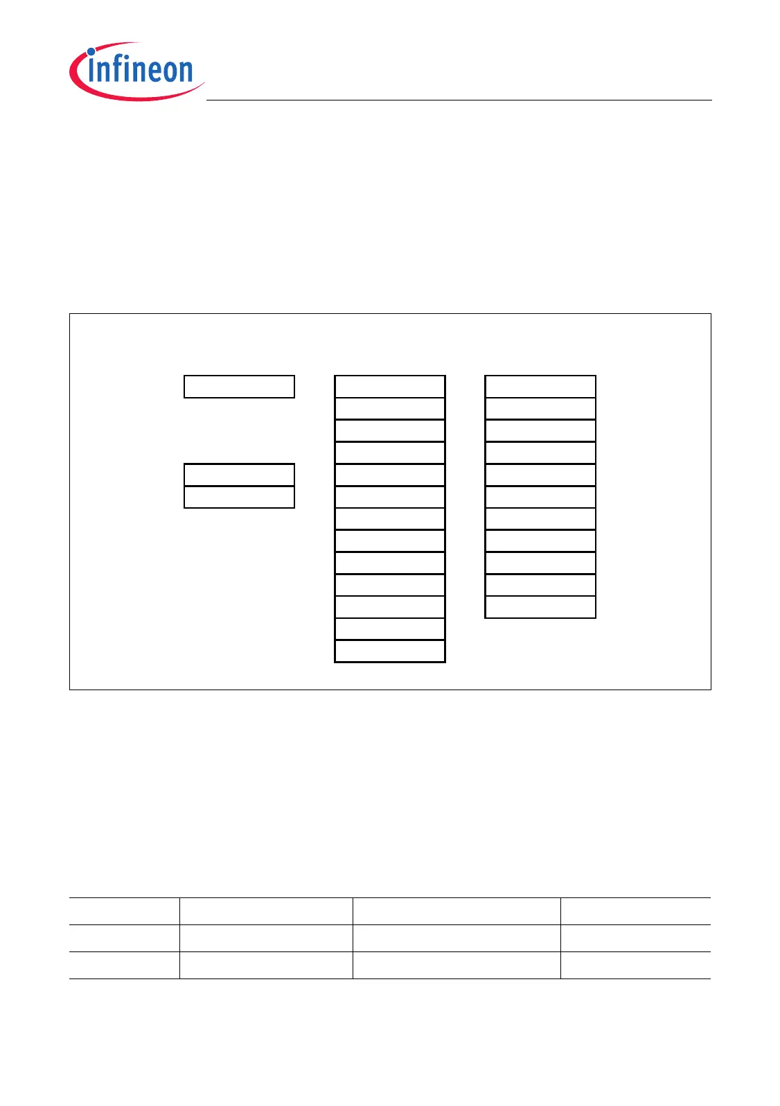
ADC Kernel Register Overview
Figure 25-29 ADC Kernel Registers
The complete and detailed address map of the ADC0 module is described in
Table 18-29 on Page 18-87 of the TC1796 User’s Manual System Units part (Volume 1).
Note: For documentation automation purposes, the CHCON and CHSTAT registers use
index "m" while LCCON registers use index "x" in the ADC module kernel register
description. These indexes are represented by "n" for CHCON and CHSTAT
registers and "m" for LCCON register in other sections of the chapter.
Table 25-12 Registers Address Space - ADC Kernel Registers
Module Base Address End Address Note
ADC0 F010 0400
H
F010 05FF
H
–
ADC1 F010 0600
H
F010 07FF
H
–
CHCONm
MCA06032_mod
CHSTATm
TTC
TCRP AP
Channel
Registers
Trigger Source
Registers
Global
Registers
TCON
TSTAT
SAL
QUEUE0
QR
EXTC
EXCRP
SCN
ASCRP
CHIN
REQ0
SW0CRP
SCON
CON
STAT
LCCONx
MSS0
MSS1
SRNP
SYSTAT
x = 0-3
m = 0-15
ID
Identification
Register
ID
 Loading...