TC1796
Peripheral Units (Vol. 2 of 2)
Analog-to-Digital Converter (ADC)
User’s Manual 25-90 V2.0, 2007-07
ADC, V2.0
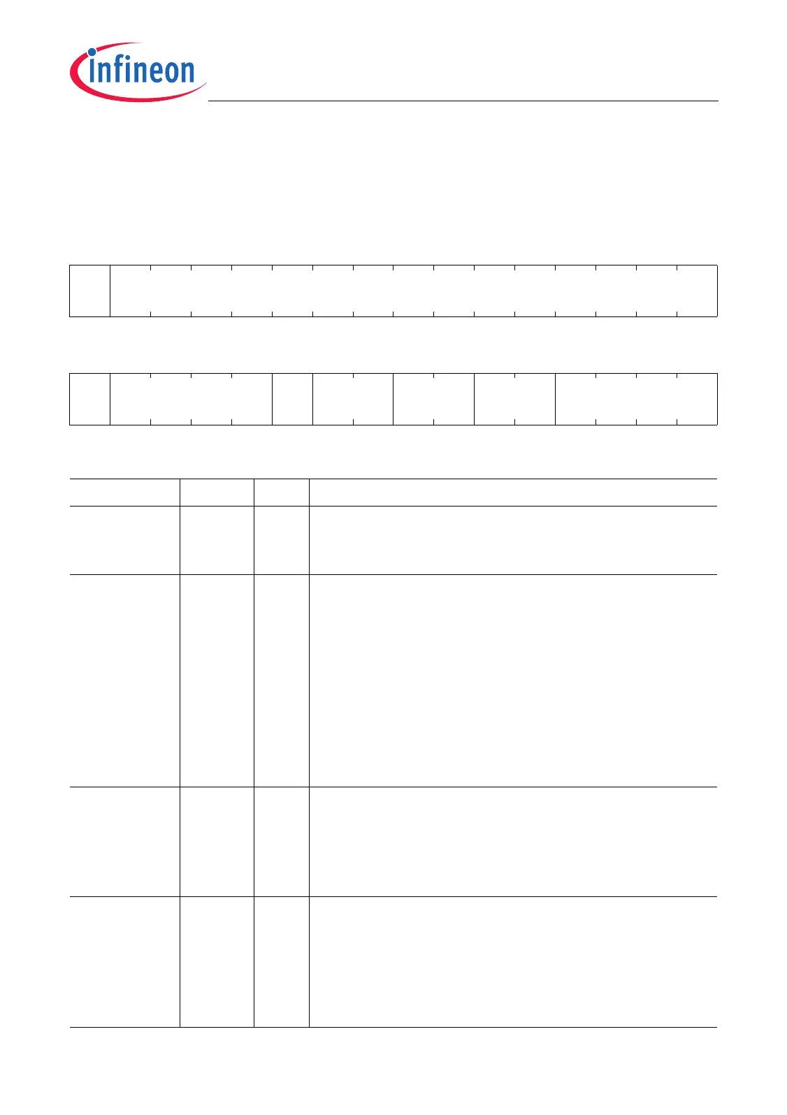
25.2.8 Channel Inject Register
CHIN
Channel Injection Control Register (118
H
) Reset Value: 0000 0000
H
31 30 29 28 27 26 25 24 23 22 21 20 19 18 17 16
CIN
REQ
0
rw r
1514131211109876543210
CIR
EN
0
GRP
S
EMUX RES 0 CHNRIN
rw r rw rw rw r rw
Field Bits Type Description
CHNRIN [3:0] rw Channel Number to be Injected
This bit field indicates the channel number of the
analog channel which is used for channel injection.
RES [7:6] rw Conversion Resolution Control
This bit field controls the resolution of the A/D
Converter for the conversion of the analog channel
determined by CHNRIN. Any modification of this bit
field is taken into account after the currently running
conversion is finished.
00
B
10-bit resolution
01
B
12-bit resolution
10
B
8-bit resolution
11
B
Reserved
EMUX [9:8] rw External Multiplexer Control
This bit indicates the settings of the external
multiplexer control lines that is used during an A/D
conversion for the analog channel determined by
CHNRIN.
GRPS 10 rw Analog Input Multiplexer Group Select
This bit selects the analog input multiplexer group for
the conversion of the analog channel determined by
CHNRIN.
0
B
Analog input multiplexer group 0 selected.
1
B
Analog input multiplexer group 1 selected.

 Loading...