TC1796
System Units (Vol. 1 of 2)
General Purpose I/O Ports and Peripheral I/O Lines
User’s Manual 10-10 V2.0, 2007-07
Ports, V2.0
Port Control Coding
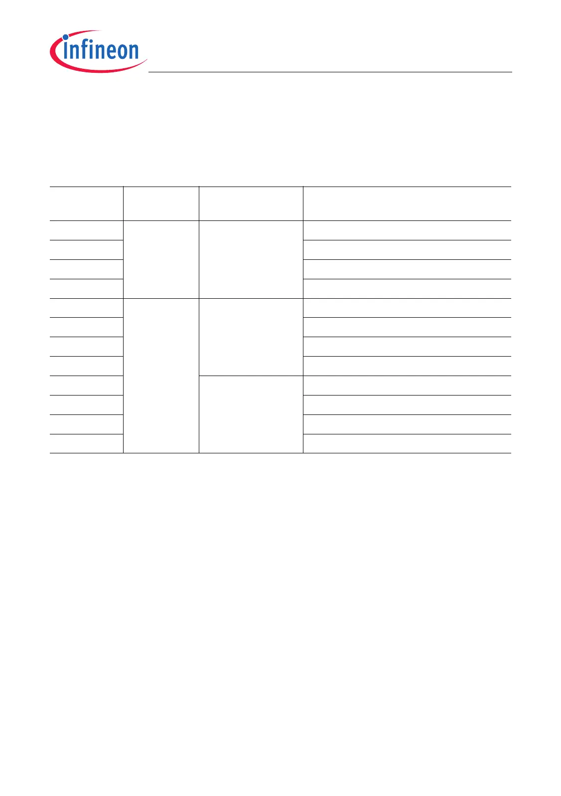
Table 10-3 describes the coding of the PCx bit fields that determine the port line
functionality.
10.2.2 Pad Driver Mode Register
Overview
The pad structure of the TC1796 GPIO lines offers the possibility to select the output
driver strength and the slew rate. These two parameters are controlled by the bit fields
in the pad driver mode register Pn_PDR, independently from input/output and pull-
up/pull-down control functionality as programmed in the Pn_IOCR register. One
Pn_PDR register is assigned to each port.
The GPIO port lines consist of by two classes of pads:
• Class A1 pins (low speed 3.3V LVTTL outputs)
• Class A2 pins (high speed 3.3V LVTTL outputs. e.g. for serial outputs)
The assignment of each port pin to one of these pad classes is shown in the port
configuration figures (Figure 10-4 to Figure 10-13). Further details about pad driver
classes that are available in the TC1796 are summarized in Table 1-5 on Page 1-57.
Table 10-3 PCx Coding (except Port 4)
PCx[3:0] I/O Output
Characteristics
Selected Pull-up / Pull-down /
Selected Output Function
0X00
B
Input – No input pull device connected
0X01
B
Input pull-down device connected
0X10
B
1)
1) This bit field value is default after reset.
Input pull-up device connected
0X11
B
No input pull device connected
1000
B
Output Push-pull General-purpose output
1001
B
Alternate output function 1
1010
B
Alternate output function 2
1011
B
Alternate output function 3
1100
B
Open-drain General-purpose output
1101
B
Alternate output function 1
1110
B
Alternate output function 2
1111
B
Alternate output function 3

 Loading...