TC1796
Peripheral Units (Vol. 2 of 2)
Analog-to-Digital Converter (ADC)
User’s Manual 25-114 V2.0, 2007-07
ADC, V2.0
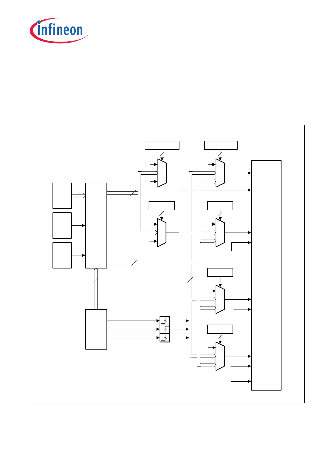
25.3.6.2 Request/Gating Input Signal Connections
The on-chip interconnections of the A/D Converters request and trigger inputs are shown
in Figure 25-34. Request and gating signals for ADC0 and ADC1, derived by pins, MSC
outputs, or GPTA outputs are generated by the External Request Unit (ERU). The ERU
is located in the System Control Unit (SCU) of the TC1796. Three output signals of
GPTA0 are able to directly trigger A/D Converter channels.
Figure 25-34 Request/Gating Input Signal Connections (ADC0/ADC1)
The signal source for trigger and gating signals of each A/D Converter, ADC0 and ADC1,
is selected via register TGADC0 and TGADC1.
ERU
MCA06037
ADCx
EGT
TGADCx
ETR
ETRSEL
SW0GT
TGADCx
SW0TR
SW0TRSEL
TGT
TGADCx
0
TTR
TTRSEL
3
QGT
TGADCx
0
QTR
QTRSEL
ASGT
TGADCx
EGTSEL
GPTA0_OUT3
GPTA0_OUT28
GPTA0_OUT11
Rising Edge
Detection
TGADCx
SW0GTSEL
PDOUT
TOUT
4
4
x = 0, 1
GPTA0
3
6
3
33
3
8
0
1
0
1
0
0
1
1
1
MSC1
MSC0
GPIO

 Loading...