TC1796
System Units (Vol. 1 of 2)
General Purpose I/O Ports and Peripheral I/O Lines
User’s Manual 10-13 V2.0, 2007-07
Ports, V2.0
Further details of the temperature compensation logic are described in Section 5.6 on
Page 5-41 (SCU) of this User’s Manual.
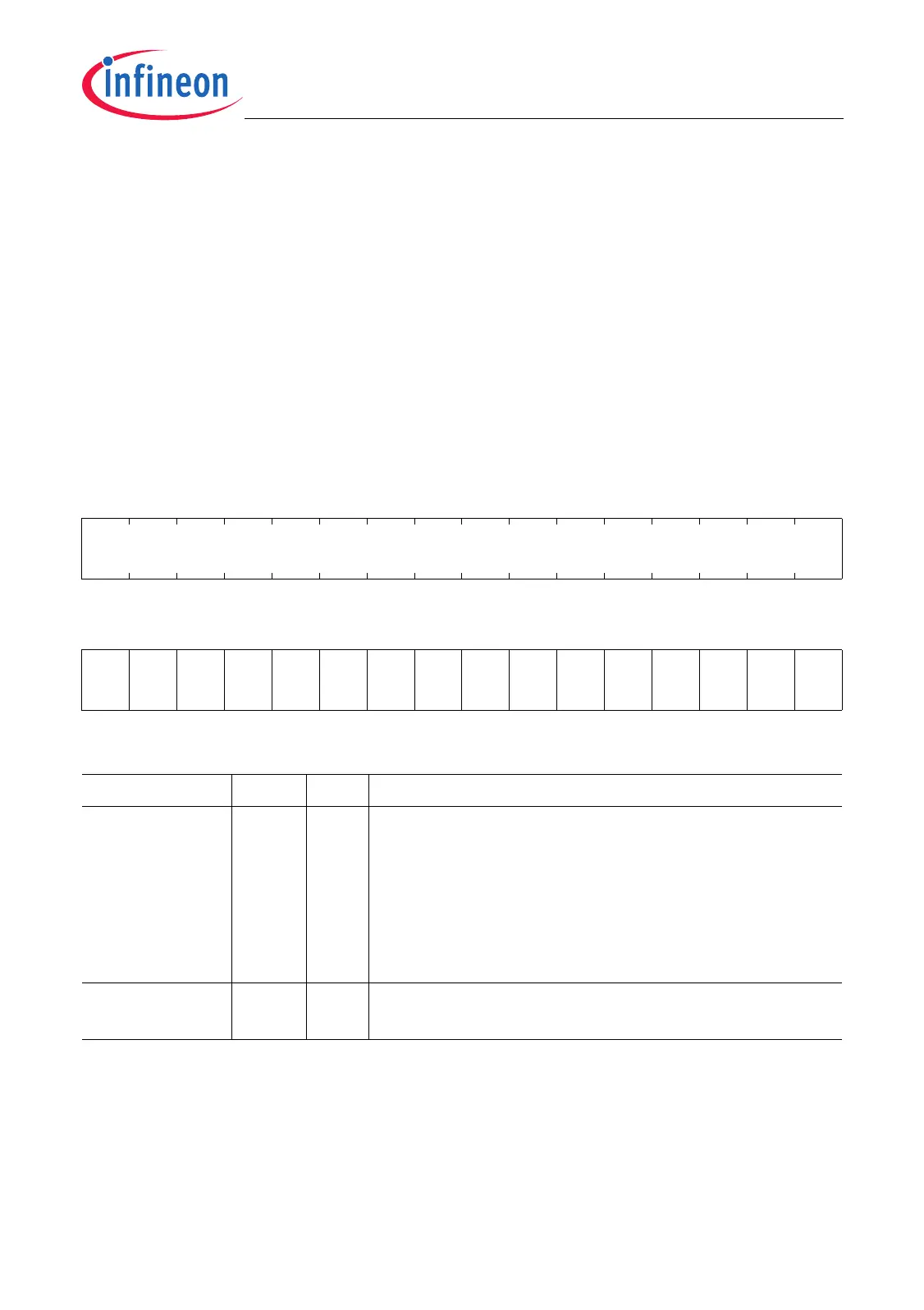
10.2.3 Port Output Register
The port output register determines the value of a GPIO pin when it is selected by
Pn_IOCRx as output. Writing a 0 to a Pn_OUT.Px (x = 0-15) bit position delivers a low
level at the corresponding output pin. A high level is output when the corresponding bit
is written with a 1. Note that the bits of Pn_OUT.Px can also be also set/cleared by
writing appropriate values into the port output modification register Pn_OMR.
Note: Only Port 0, 1, 3, and 4 are 16-bit wide ports. The Pn_OUT registers of the other
ports have a reduced number of Px bits (see Pn_OUT register descriptions in the
corresponding port sections).
Pn_OUT
Port n Output Register (00
H
) Reset Value: 0000 0000
H
31 30 29 28 27 26 25 24 23 22 21 20 19 18 17 16
0
r
1514131211109876543210
P15 P14 P13 P12 P11 P10 P9 P8 P7 P6 P5 P4 P3 P2 P1 P0
rwh rwh rwh rwh rwh rwh rwh rwh rwh rwh rwh rwh rwh rwh rwh rwh
Field Bits Type Description
Px
(x = 0-15)
xrwhPort n Output Bit x
This bit determines the level at the output pin Pn.x if
the output is selected as GPIO output.
0
B
The output level of Pn.x is 0.
1
B
The output level is Pn.x is 1.
Pn.x can also be set/cleared by control bits of the
Pn_OMR register.
0 [31:16] r Reserved
Read as 0; should be written with 0.

 Loading...