TC1796
System Units (Vol. 1 of 2)
General Purpose I/O Ports and Peripheral I/O Lines
User’s Manual 10-57 V2.0, 2007-07
Ports, V2.0
10.8.3 Port 5 Registers
The following registers are available on Port 5:
Note: The complete address map of Port 5 is described in Table 18-14 on Page 18-27
of this TC1796 System Units (Vol. 1 of 2) User’s Manual.
10.8.3.1 Port 5 Output Register
The basic P5_OUT register functionality is described on Page 10-13. Port lines P5.[15:8]
are not available. Therefore, the P5_OUT bits P[15:8] should be written with 0, and are
always read as 0.
10.8.3.2 Port 5 Output Modification Register
The basic P5_OMR register functionality is described on Page 10-14. Port lines
P5.[15:8] are not available. Therefore, the P5_OMR bits PS[15:8] and PR[15:8] are not
implemented. These bits should always be written with 0.
10.8.3.3 Port 5 Input Register
The basic P5_IN register functionality is described on Page 10-17. Port lines P5.[15:8]
are not available. Therefore, the P5_IN bits P[15:8] are always read as 0.
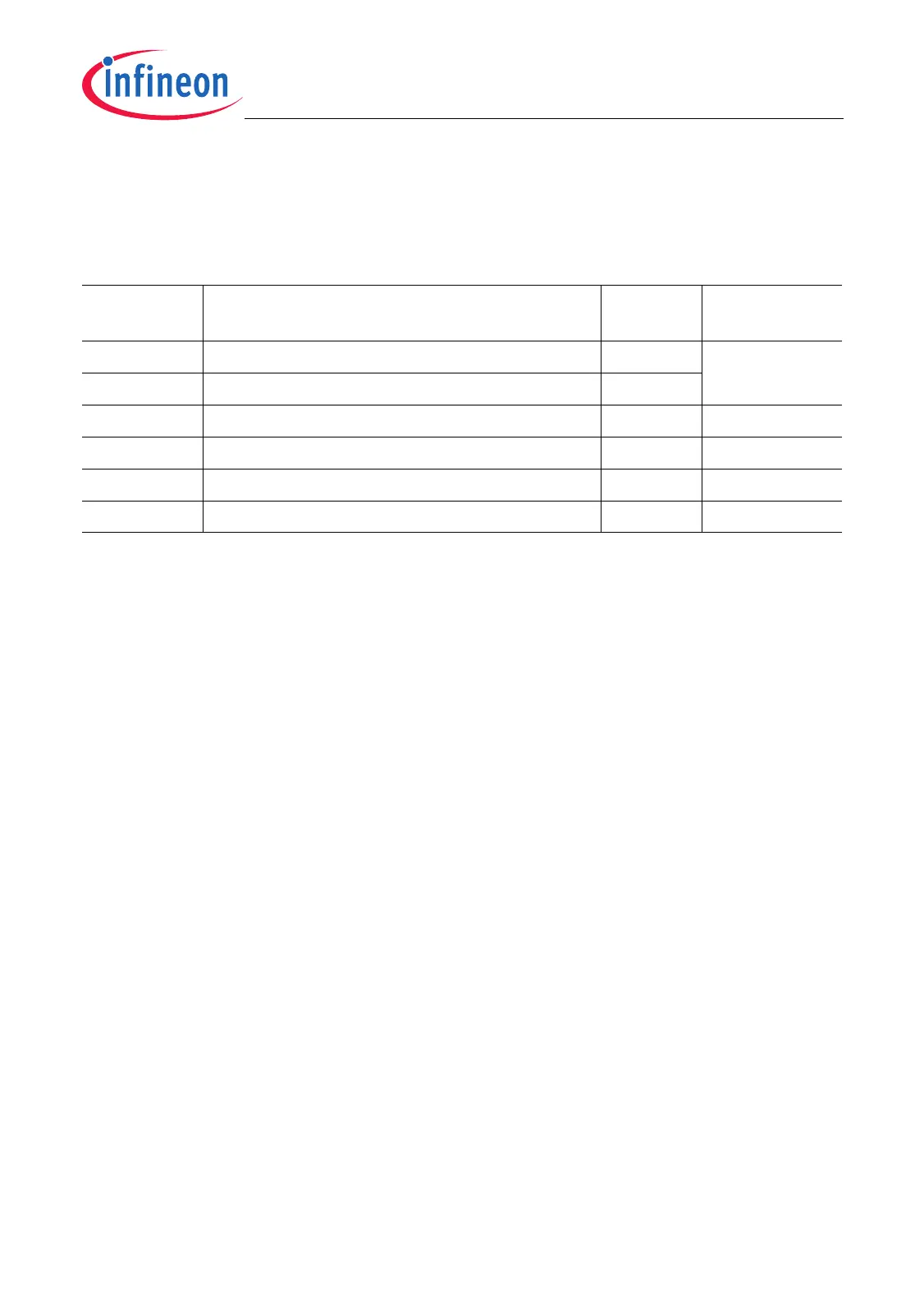
Table 10-18 Port 5 Registers
Register
Short Name
Register Long Name Offset
Address
Description
see
P5_OUT Port 5 Output Register 0000
H
below
1)
1) These registers are noted here in the Port 5 section because they differ from the general port register
description given in Section 10.2.
P5_OMR Port 5 Output Modification Register 0004
H
P5_IOCR0 Port 5 Input/Output Control Register 0 0010
H
Page 10-8
P5_IOCR4 Port 5 Input/Output Control Register 4 0014
H
Page 10-8
P5_IN Port 5 Input Register 0024
H
below
1)
P5_PDR Port 5 Pad Driver Mode Register 0040
H
Page 10-58
1)

 Loading...