TC1796
Peripheral Units (Vol. 2 of 2)
General Purpose Timer Array (GPTA)
User’s Manual 24-267 V2.0, 2007-07
GPTA, V2.0
24.6.5.1 Clock Control Registers
The clock control register makes it possible to control (enable/disable) the module
control clock f
CLC
. The clock signal f
CLC
is used by the GPTA0, GPTA1, and LTCA2 as a
clock for internal control operations but not for timer purposes.
Note: After a hardware reset operation, the f
CLC
clock is disabled (DISS set). Therefore,
the GPTA modules clock generation is completely disabled.
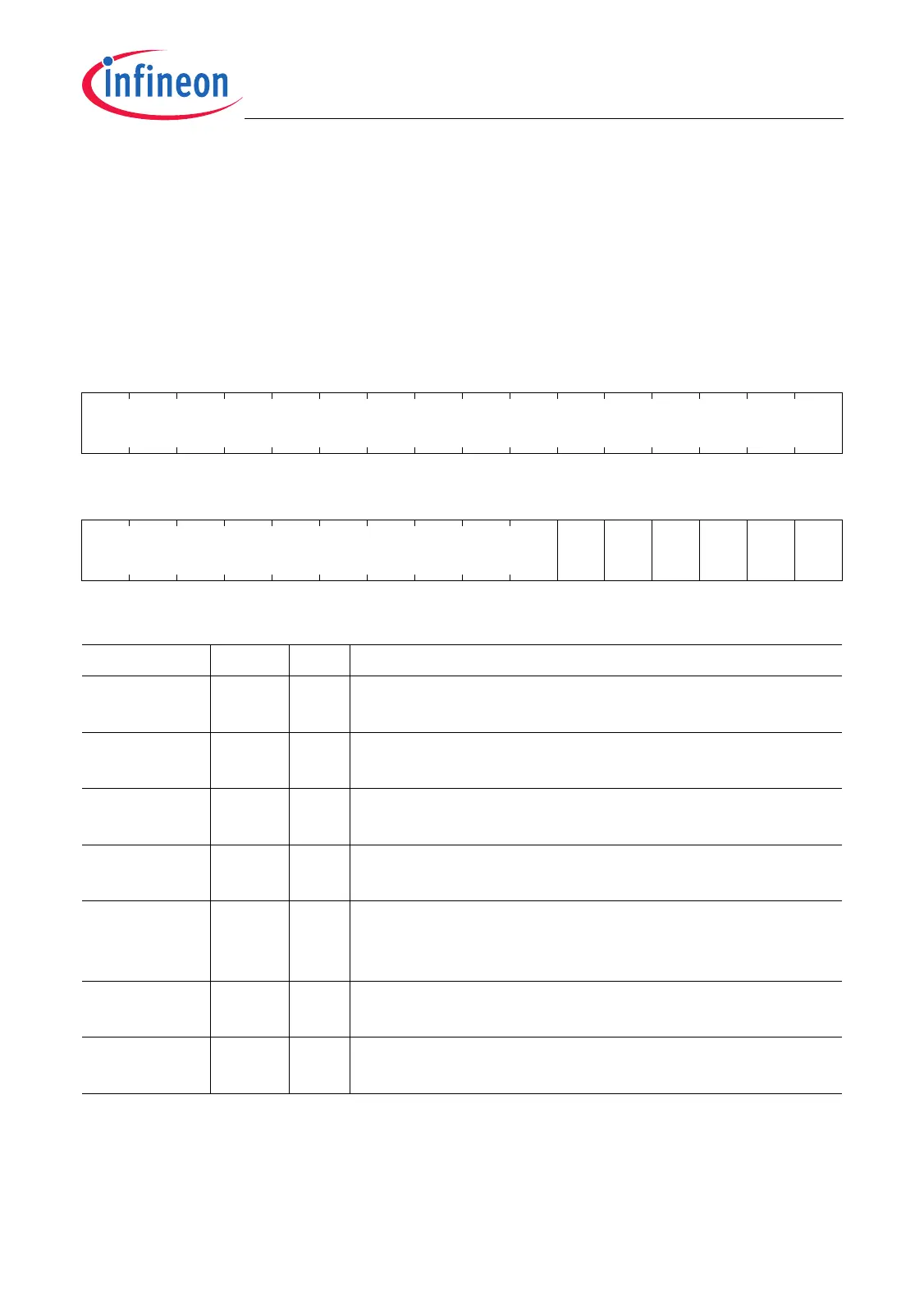
GPTA0_CLC
GPTA Clock Control Register (000
H
) Reset Value: 0000 0003
H
31 30 29 28 27 26 25 24 23 22 21 20 19 18 17 16
0
r
1514131211109876543210
0
FS
OE
SB
WE
E
DIS
SP
EN
DIS
S
DIS
R
rrwwrwrwrrw
Field Bits Type Description
DISR 0rwModule Disable Request Bit
Used for enable/disable control of the module.
DISS 1rModule Disable Status Bit
Bit indicates the current status of the module.
SPEN 2rwModule Suspend Enable for OCDS
Used to enable the suspend mode.
EDIS 3rwExternal Request Disable
Used to control the external clock disable request.
SBWE 4wModule Suspend Bit Write Enable for OCDS
Determines whether SPEN and FSOE are write-
protected.
FSOE 5rwFast Switch Off Enable
Used for fast clock switch off in suspend mode.
0 [31:6] r Reserved
Read as 0; should be written with 0.
 Loading...