TC1796
Peripheral Units (Vol. 2 of 2)
Analog-to-Digital Converter (ADC)
User’s Manual 25-33 V2.0, 2007-07
ADC, V2.0
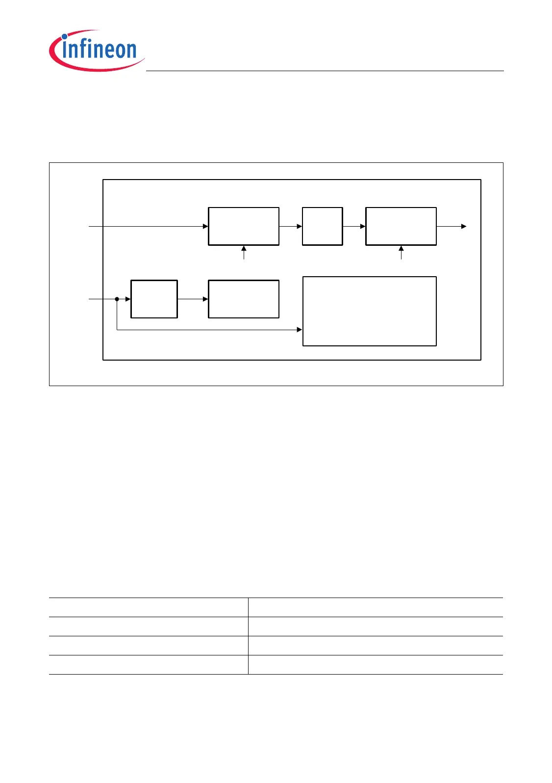
25.1.4 Clock Circuit
The clock divider blocks shown in Figure 25-18 determine the clock frequencies in the
ADC module and the conversion and sample timing.
Figure 25-18 Clock Control Structure
The following definitions for the A/D Converter clocks are used in this chapter:
• f
CLC
: Module control clock
• f
ADC
: Module timing clock
• f
BC
: Basic operating clock
• f
ANA
: Internal A/D Converter clock
• f
TIMER
: Arbiter clock
The conversion time is composed of the sample time, the time for the successive
approximation, and the calibration time. Table 25-6 shows the conversion time t
C
based
on the sample time t
S
, basic operating clock frequency f
BC
and the module timing clock
f
ADC
(t
BC
= 1 / f
BC
, t
ADC
= 1 / f
ADC
).
Note: The TC1796 basic operating clock frequency f
BC
influences the maximum
allowable internal resistance of the used reference voltage supply.
Table 25-6 Conversion Time t
C
A/D Converter Resolution Conversion Time t
C
8-bit t
S
+ 40 t
BC
+ 2 t
ADC
10-bit t
S
+ 48 t
BC
+ 2 t
ADC
12-bit t
S
+ 56 t
BC
+ 2 t
ADC
MCA06021
Programmable
Clock Divider
(1:1) to (1:256)
f
BC
f
ADC
f
ANA
Programmable
Counter
Sample
Time
t
S
CON.CTC CHCONn.STC
f
TIMER
Control/Status Logic
Interrupt Logic
External Trigger Logic
External Multiplexer Logic
Request Generation Logic
A/D Converter Module
Arbiter
(1:20)
Control Unit
(Timer)
1:4
f
CLC
 Loading...