TC1796
System Units (Vol. 1 of 2)
Direct Memory Access Controller
User’s Manual 12-111 V2.0, 2007-07
DMA, V2.0
12.4.2 Registers
This section describes the kernel registers of the Memory Checker module.
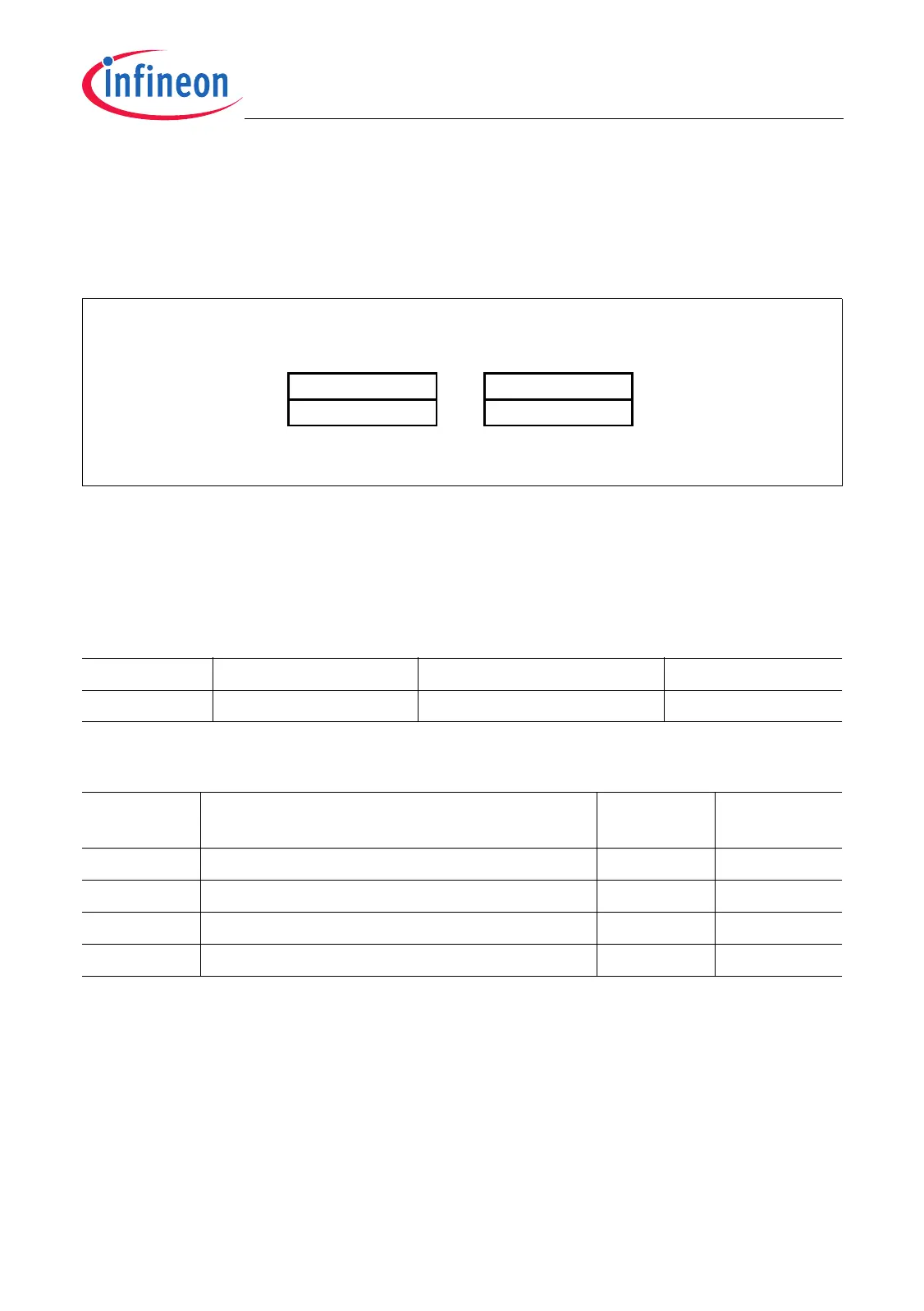
MCHK Register Overview
Figure 12-34 Memory Checker Registers
The complete and detailed address map of the of the Memory Checker module is
described in Table 18-31 on Page 18-103 of the TC1796 User’s Manual System Units
part (Volume 1).
Table 12-15 Registers Address Space - Memory Checker
Module Base Address End Address Note
MCHK F010 C200
H
F010 C2FF
H
–
Table 12-16 Registers Overview - Memory Checker egisters
Register
Short Name
Register Long Name Offset
Address
1)
1) The absolute register address is calculated as follows:
Module Base Address (Table 12-5) + Offset Address (shown in this column)
Description
see
MCHK_ID Memory Checker Module Identification Reg. 0008
H
Page 12-112
MCHK_IR Memory Checker Input Register 0010
H
Page 12-113
MCHK_RR Memory Checker Result Register 0014
H
Page 12-113
MCHK_WR Memory Checker Write Register 0020
H
Page 12-114
MCA05711_mod
Memory Checker
Registers
MCHK_IR
MCHK_RR MCHK_WR
Other Registers
MCHK_ID

 Loading...