TC1796
System Units (Vol. 1 of 2)
Direct Memory Access Controller
User’s Manual 12-114 V2.0, 2007-07
DMA, V2.0
The Memory Checker Write Register is a dummy write-only register that is located within
the memory checker address range. This register is near by (above) the MLI address
range of the TC1796. It has no meaning for memory checker operation.
The Memory Checker Write Register can be used as dummy write register at the write
back action of the DMA or MLI controller Move Engines when the pattern detection
feature of the DMA controller is used. Accessing MCHK_WR with the Move Engines of
the MLI or DMA controller via the Bus Switch of the DMA controller (see Figure 12-14)
does not request the two FPI buses of the TC1796, SPB and RPB, because it is near the
MLI modules address ranges.
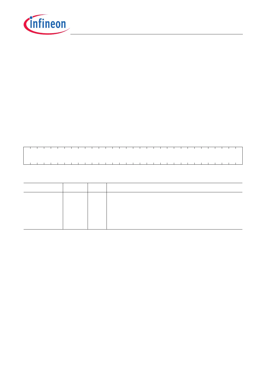
MCHK_WR
Memory Checker Write Register (20
H
) Reset Value: 0000 0000
H
31 0
WO
w
Field Bits Type Description
WO [31:0] w Write-Only
This write-only bit field is used to write dummy data
during DMA pattern detection. The data written to
WO is not taken into account for any action. Any read
action of WO will deliver 0000 0000
H
.

 Loading...