TC1796
System Units (Vol. 1 of 2)
Direct Memory Access Controller
User’s Manual 12-113 V2.0, 2007-07
DMA, V2.0
The Memory Checker Input Register is used during write moves of a memory checker
related DMA transaction as data destination with its fixed register address. If the DMA
moves to register MCHK_IR are 8-bit or 16-bit wide, the unused register bits of the 32-bit
MCHKIN value are taken as 0s for the current result calculation.
Note: MCHK_IR is a write-only register. Any read action will deliver 0000 0000
H
.
The Memory Checker Result Register contains the result of the memory check
operation. Before starting a checksum calculation operation, it should be written with an
initial checksum calculation value.
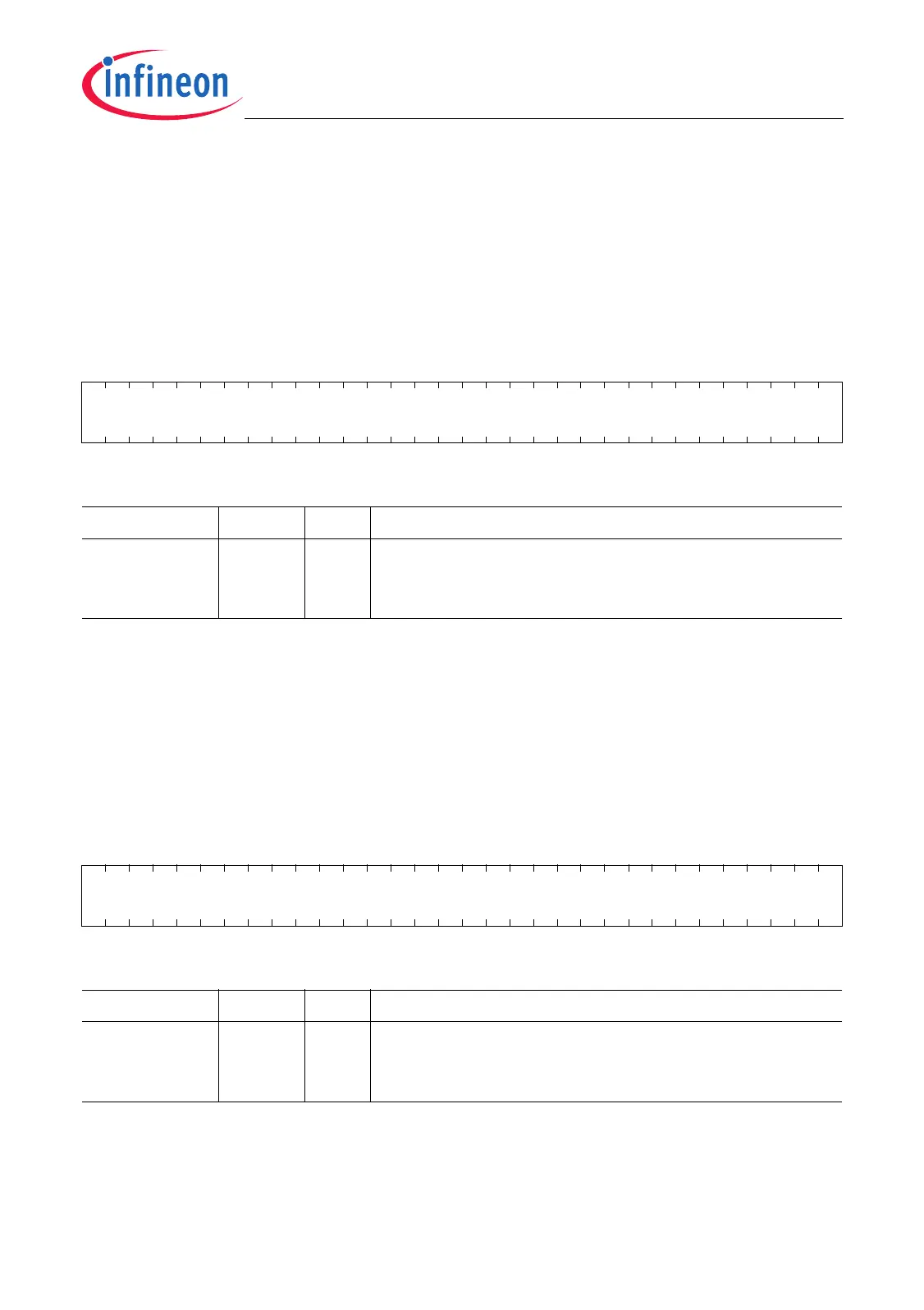
MCHK_IR
Memory Checker Input Register (10
H
) Reset Value: 0000 0000
H
31 0
MCHKIN
w
Field Bits Type Description
MCHKIN [31:0] w Memory Checker Input
The value written to MCHKIN is used for the next
checksum calculation. Any read action will deliver 0.
MCHK_RR
Memory Checker Result Register (14
H
) Reset Value: 0000 0000
H
31 0
MCHKR
rwh
Field Bits Type Description
MCHKR [31:0] rwh Memory Checker Result
This bit field contains the current result of the memory
checksum calculation operation.

 Loading...