TC1796
Peripheral Units (Vol. 2 of 2)
General Purpose Timer Array (GPTA)
User’s Manual 24-265 V2.0, 2007-07
GPTA, V2.0
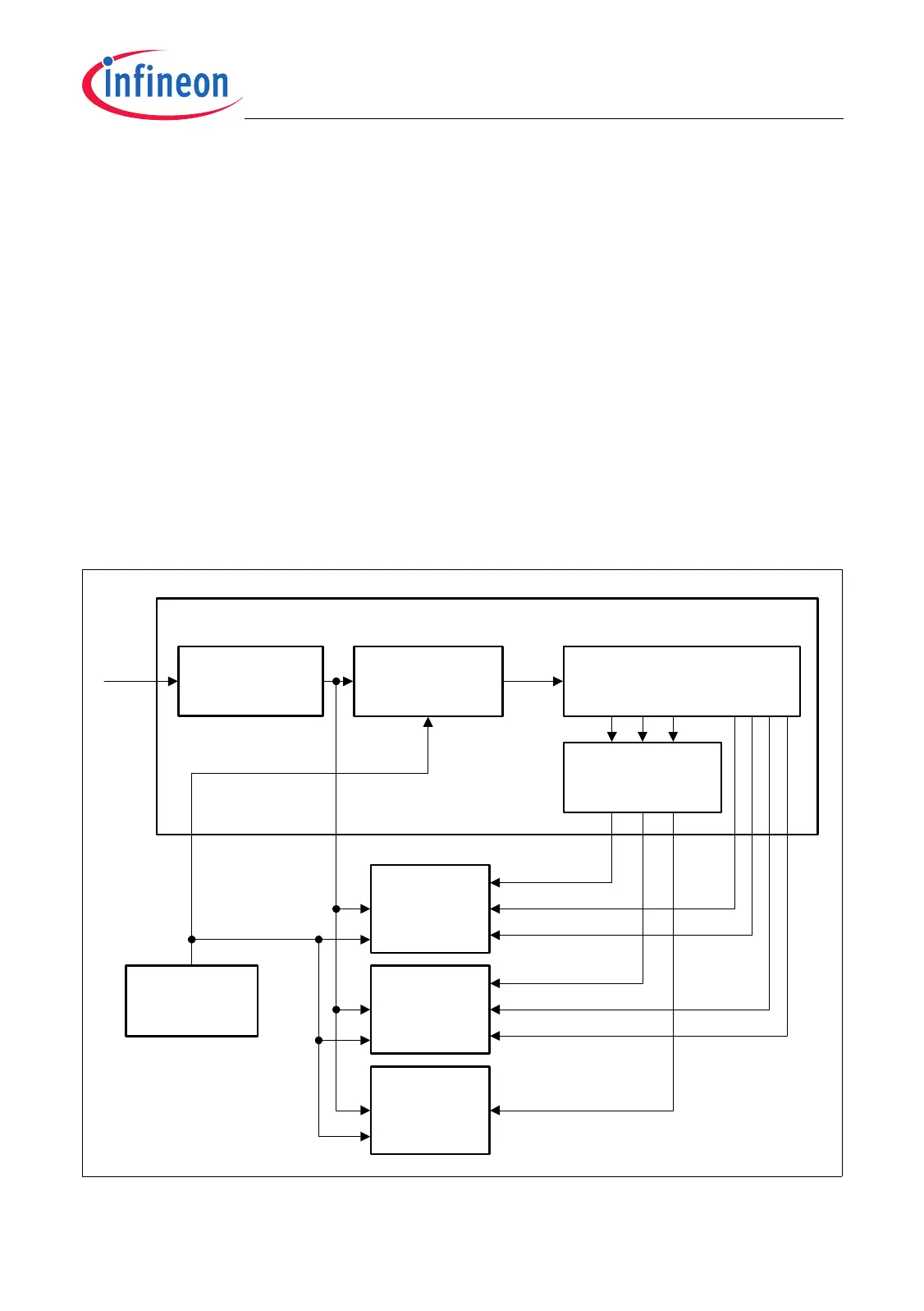
24.6.5 Module Clock Generation
As shown in Figure 24-92, the clock signals for the GPTA0, GPTA1, and LTCA2
modules are generated and controlled by one clock generation unit. This clock
generation unit is responsible for the enable/disable control, the clock frequency
adjustment, and the debug clock control. The unit includes four registers:
• Clock Control Register GPTA0_CLC (see Page 24-267),
responsible for the generation of the control clock
f
CLC
that is used by each of the
three kernel modules as general control tasks.
• Fractional Divider Register GPTA0_FDR (see Page 24-268),
responsible for the frequency control of the module timer clock
f
GPTA
.
• Clock Enable/Disable Control Register GPTA0_EDCTR (see Page 24-270),
responsible for the enable/disable control of the three module timer clocksf
GPTA0
,
f
GPTA1
, and f
LTCA2
, and for the run control for the Global Timers in GPTA0 and GPTA1.
• Debug Clock Control Register GPTA0_DBGCTR (see Page 24-271),
responsible for the module timer clock control in Debug Mode.
Figure 24-92 GPTA Modules Clock Generation
MCA06001
Clock Control
Register
GPTA0_CLC
f
CLC
Fractional Divider
Register
GPTA0_FDR
Clock Generation Unit for GPTA Modules
Clock Enable/Disable
Control Register
GPTA0_EDCTR
f
GPTA
f
GPTA0
f
GPTA1
f
LTCA2
GPTA0
Kernel
f
SYS
GPTA1
Kernel
LTCA2
Kernel
GT00RUN
GT01RUN
GT10RUN
GT11RUN
(used for control
tasks and register
accesses)
Debug Clock
Control Register
GPTA0_DBGCTR
MultiCAN
Module
SR15
ECEN
INT0
INT0
INT0

 Loading...