TC1796
System Units (Vol. 1 of 2)
Clock System and Control
User’s Manual 3-39 V2.0, 2007-07
Clock, V2.0
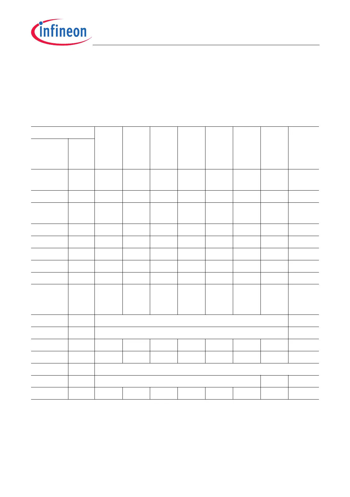
3.3.4 Module Clock Register Implementations
Table 3-9 shows which of the CLC register bits/bit fields are implemented for each
peripheral module in the TC1796 and which modules are equipped with a fractional
divider.
Note: The ports of the TC1796, SCU, and WDT do not provide CLC registers.
Table 3-9 Clock Generation Implementation of the TC1796 Peripheral Modules
Module DISR
Bit 0
DISS
Bit 1
SPEN
Bit 2
EDIS
Bit 3
SBWE
Bit 4
FSOE
Bit 5
RMC Fract.
Divider
1)
1) Further info on FDR implementations see Table 3-10.
Name State
after
Reset
ADC0
ADC1
off ✔✔✔✔✔✔– ✔
FADC off ✔✔✔✔✔✔– ✔
ASC0 and
ASC1
off ✔✔✔✔✔✔8-bit –
SSC0 off ✔✔✔✔✔✔– ✔
SSC1 off ✔✔✔✔✔✔– ✔
MultiCAN off ✔✔✔✔✔✔– ✔
DMA on ✔✔✔✔✔✔––
EBU on ✔✔––––––
GPTA0
GPTA1
LTCA2
off ✔✔✔✔✔✔– ✔
MLI0 off not implemented, MLI is connected to DMA_CLC ✔
MLI1 off not implemented, MLI is connected to DMA_CLC ✔
MSC0 off ✔✔✔✔✔✔– ✔
MSC1 off ✔✔✔✔✔✔– ✔
PCP2 off different bit definitions
2)
2) Automatic clock switch-off capability if PCP is idle.
PLL on different bit definitions – –
STM on ✔✔✔✔✔✔3-bit –

 Loading...