TC1796
System Units (Vol. 1 of 2)
General Purpose I/O Ports and Peripheral I/O Lines
User’s Manual 10-30 V2.0, 2007-07
Ports, V2.0
10.4.3 Port 1 Registers
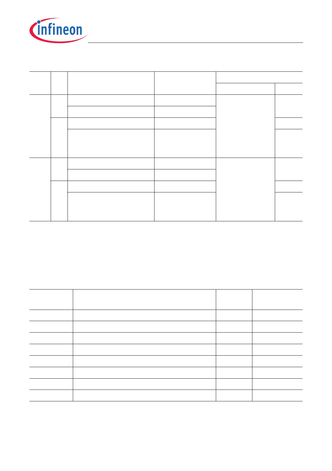
The following registers are available on Port 1:
P1.14 I General-purpose input P1_IN.P14 P1_IOCR12.
PC14
0XXX
B
MLI0 input RVALID0B
O General-purpose output P1_OUT.P14 1X00
B
Reserved
1)
–1X01
B
1X10
B
1X11
B
P1.15 I General-purpose input P1_IN.P15 P1_IOCR12.
PC15
0XXX
B
MLI0 input RDATA0B
O General-purpose output P1_OUT.P15 1X00
B
Reserved
1)
–1X01
B
1X10
B
1X11
B
1) The port I/O control values P1_IOCRx.Py that are assigned to this reserved alternate output control selection
should not be used. Otherwise, unpredictable output port line behavior may occur.
Table 10-10 Port 1 Registers
Register
Short Name
Register Long Name Offset
Address
Description
see
P1_OUT Port 1 Output Register 0000
H
Page 10-13
P1_OMR Port 1 Output Modification Register 0004
H
Page 10-14
P1_IOCR0 Port 1 Input/Output Control Register 0 0010
H
Page 10-7
P1_IOCR4 Port 1 Input/Output Control Register 4 0014
H
Page 10-8
P1_IOCR8 Port 1 Input/Output Control Register 8 0018
H
Page 10-8
P1_IOCR12 Port 1 Input/Output Control Register 12 001C
H
Page 10-9
P1_IN Port 1 Input Register 0024
H
Page 10-17
P1_PDR Port 1 Pad Driver Mode Register 0040
H
Page 10-31
1)
1) This register is listed here in the Port 1 section because they differ from the general port register description
given in Section 10.2.
Table 10-9 Port 1 Functions (cont’d)
Port
Pin
I/O Pin Functionality Associated Reg./
I/O Line
Port I/O Control Select.
Reg./Bit Field Value

 Loading...