TC1796
System Units (Vol. 1 of 2)
On-Chip Debug Support
User’s Manual 17-8 V2.0, 2007-07
OCDS, V2.0
17.2.1.4 TriCore OCDS Registers
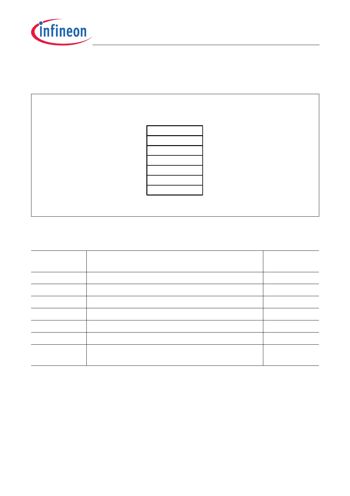
Figure 17-4 shows the TriCore OCDS registers in an overview.
Figure 17-4 TriCore Core Debug Registers
17.2.2 PCP OCDS Level 1
The PCP has no means for generating trigger events. To set breakpoints the debugger
is expected to patch the code in the PCP code memory (CMEM) with DEBUG
instructions.
If a DEBUG instruction is executed, the running channel program is terminated, either
with Debug Exit or with Error Exit. Additionally the Break Switch can send an external
break request to the PCP, with the same consequence (Debug Exit or Error Exit).
Table 17-1 TriCore OCDS Registers
Register
Short Name
Register Long Name Address
DBGSR Debug Status Register F7E1 FD00
H
EXEVT External Break Input Event Specifier Register F7E1 FD08
H
CREVT Core SFR Access Break Event Specifier Register F7E1 FD0C
H
SWEVT Software Break Event Specifier Register F7E1 FD10
H
TR0EVT Trigger Event 0 Specifier Register F7E1 FD20
H
TR1EVT Trigger Event 1 Specifier Register F7E1 FD24
H
CPU_SBSRC0 CPU Software Break Service Request Control
Register 0
F7E0 FFBC
H
1)
1) Located in the CPU slave (CPS) interface register area.
MCA05759
DBGSR
CPU OCDS
Registers
EXEVT
CREVT
SWEVT
TR0EVT
TR1EVT
CPU_SBSRC0

 Loading...