TC1796
Peripheral Units (Vol. 2 of 2)
General Purpose Timer Array (GPTA)
User’s Manual 24-239 V2.0, 2007-07
GPTA, V2.0
24.5.6 Multiplexer Control Registers
Note: These registers are not directly accessible and can be written and read only via
the multiplexer register array FIFO.
24.5.6.1 Output Multiplexer Control Registers
Two registers, OMCRL and OMCRH, are assigned to each I/O Group IOG[4:0] and each
Output Group OG[6:0]. OMCRL[4:0]/OMCRH[4:0] are assigned to IOG[4:0] and
OMCRL[13:7]/OMCRH[13:7] are assigned to OG[6:0].
OMCRL controls the connections of group pins 0 to 3. OMCRH controls the connections
of group pins 4 to 7.
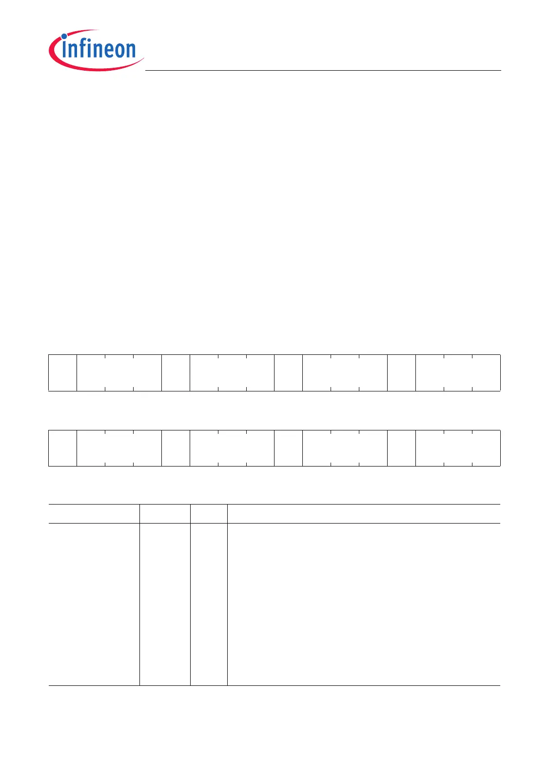
OMCRLg (g = 0-4, 7-13)
Output Multiplexer Control Register for Lower Half of Pin Group g
Reset Value: 0000 0000
H
31 30 29 28 27 26 25 24 23 22 21 20 19 18 17 16
0OMG30OML30OMG20OML2
rrwrrwrrwrrw
1514131211109876543210
0OMG10OML10OMG00OML0
rrwrrwrrwrrw
Field Bits Type Description
OML0,
OML1,
OML2,
OML3
[2:0],
[10:8],
[18:16],
[26:24]
rw Multiplexer Line Selection
This bit field selects the input line of a OMG that can
be selected by bit field OMGn for OMG output n.
000
B
000
B
OMG input IN0 selected
001
B
OMG input IN1 selected
010
B
OMG input IN2 selected
011
B
OMG input IN3 selected
100
B
OMG input IN4 selected
101
B
OMG input IN5 selected
110
B
OMG input IN6 selected
111
B
OMG input IN7 selected

 Loading...