TC1796
Peripheral Units (Vol. 2 of 2)
Micro Link Interface (MLI)
User’s Manual 23-137 V2.0, 2007-07
MLI, V2.0
23.5.4.3 Pad Driver Characteristics Selection
The Port 1, Port 5 and Port 8 pad driver mode registers contain bit fields that determine
the output driver strength and the slew rate of the MLI output lines. A detailed description
of all available PDx bit field combinations is given in Chapter “GPIO Ports” in the TC1796
System Units User’s Manual. Shaded bits and bit fields are “don’t care” for MLI0/MLI1
I/O port control purposes.
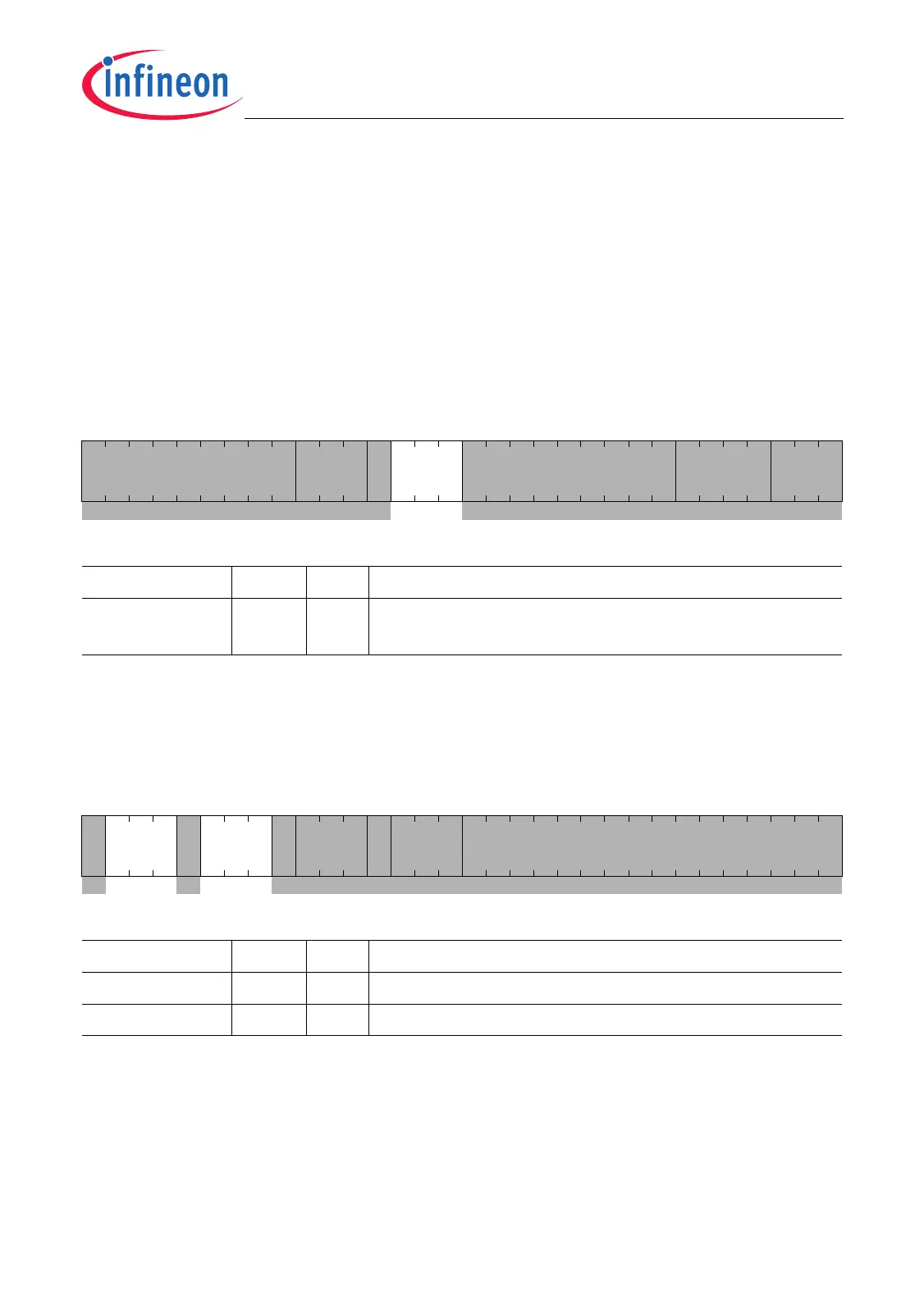
P1_PDR
Port 1 Pad Driver Mode Register (40
H
) Reset Value: 0000 0000
H
31 23 22 20 19 18 16 15 8 7 5 4 3 0
0
PDSYS
CLK
0
PD
MLI0
0
PD1
0
PD0
r rw rrw r rw rw
Field Bits Type Description
PDMLI0 [18:16] rw Pad Driver Mode for P1.4/TCLK0, P1.6/TVALID0A,
P1.7/TDATA0, and P1.9/RREADY0A
1)
1) Coding of bit field see Table 23-13. Shaded bits and bit fields are “don’t care” for MLI I/O port control.
P5_PDR
Port 5 Pad Driver Mode Register (40
H
) Reset Value: 0000 0000
H
31 30 28 27 26 24 23 22 20 19 18 16 15 0
0
PD
MSC1
0
PD
MSC0
0
PD
ASC1
0
PD
ASC0
0
rrwrrwr rw r rw r
Field Bits Type Description
PDMSC0 [26:24] rw Pad Driver Mode for P5.4/RREADY0B
1)
1) Coding of bit field see Table 23-13. Shaded bits and bit fields are “don’t care” for MLI I/O port control.
PDMSC1 [30:28] rw Pad Driver Mode for P5.6/TVALID0B
1)

 Loading...