TC1796
System Units (Vol. 1 of 2)
CPU Subsystem
User’s Manual 2-13 V2.0, 2007-07
CPU, V2.0
2.4.2 CPU Slave Interface (CPS) Registers
In the TC1796, the CPU Slave Interface (CPS) of the TriCore CPU directly accesses the
interrupt service request registers in the CPU from the TC1796 System Peripheral Bus.
The CPS registers are described in detail in the TriCore 1 Architecture Manual - Core
Registers.
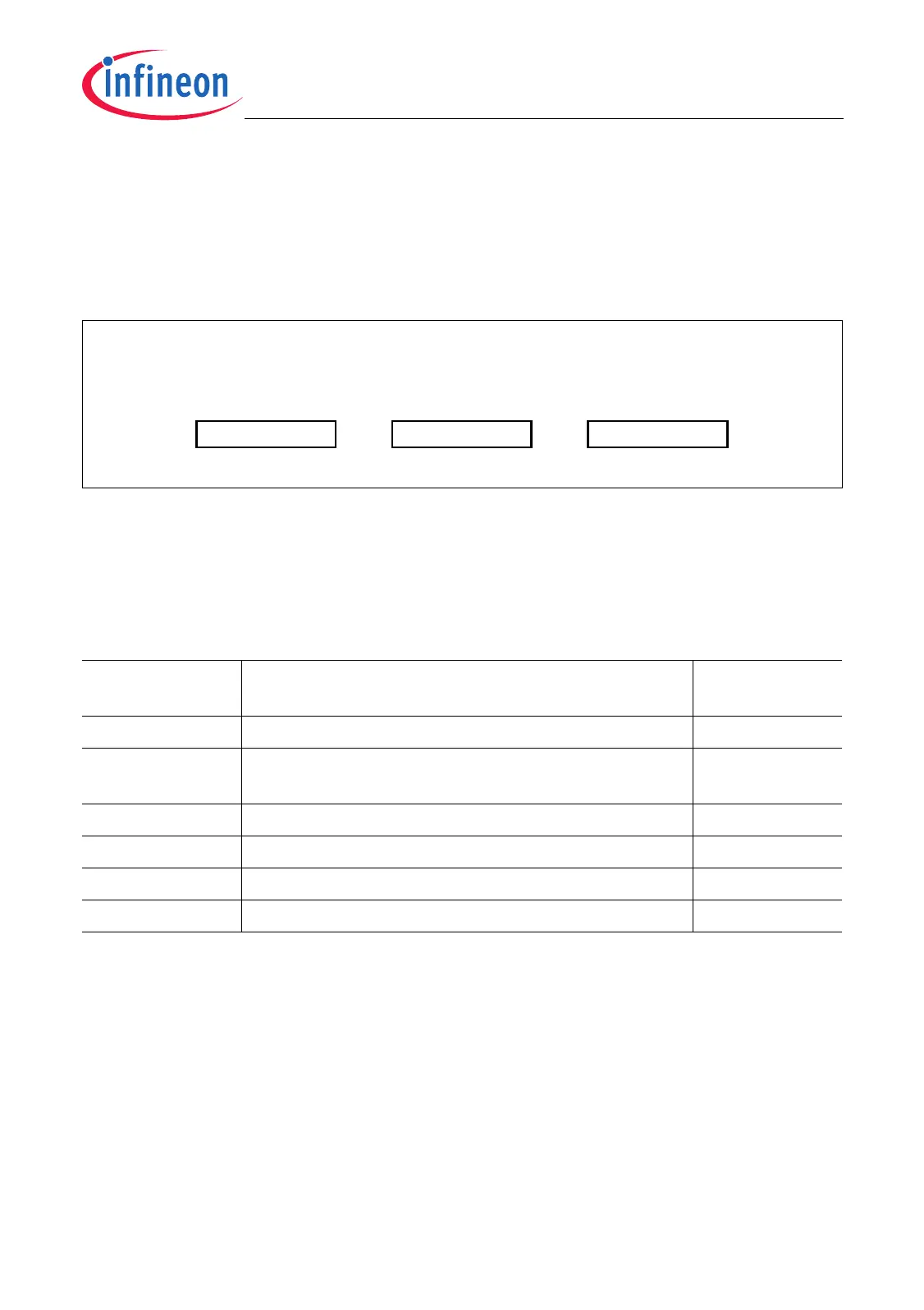
Figure 2-7 CPS Registers
The absolute register addresses are calculated by adding the offset addresses from
Table 2-3 to the CPS Base Address. The registers CPU_SBSRC0 and CPU_SRC[3:0]
are not bit-addressable.
Table 2-3 CPS Registers
Register Short
Name
Register Long Name Address
CPS_ID CPS Module Identification Register F7E0 FF08
H
CPU_SBSRC0
1)
1) CPU_SBSRC[3:1] are not implemented in the TC1796. Implementation-specific details see Page 2-19.
CPU Software Breakpoint Service Request Control
Register 0
F7E0 FFBC
H
CPU_SRC3 CPU Service Request Control Register 3 F7E0 FFF0
H
CPU_SRC2 CPU Service Request Control Register 2 F7E0 FFF4
H
CPU_SRC1 CPU Service Request Control Register 1 F7E0 FFF8
H
CPU_SRC0 CPU Service Request Control Register 0 F7E0 FFFC
H
MCA05591_mod
CPU_SBSRC0
Software Breakpoint
Service Request
Control Register
CPU Service
Request Control
Registers
(n = 3-0)
CPU_SRCnCPS_ID
Module
Identification
Register

 Loading...