TC1796
System Units (Vol. 1 of 2)
Clock System and Control
User’s Manual 3-23 V2.0, 2007-07
Clock, V2.0
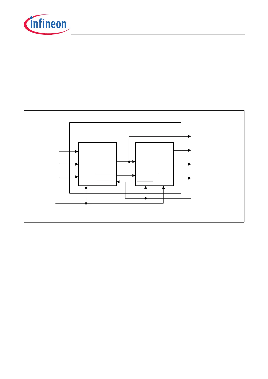
3.3.1 Module Clock Generation
As shown in Figure 3-5, module clock generation of the TC1796 on-chip modules have
two registers implemented:
• Clock Control Register CLC
• Fractional Divider Register FDR
The following sections describes the general functionality of CLC and FDR. The module-
specific implementation details are described in the corresponding module chapters.
Figure 3-5 Module Clock Generation
Module clock and CLC clock are both derived from the system clock f
SYS
. The CLC
register provides the f
CLC
clock which acts as clock input for the fractional divider and
control logic. The CLC clock f
CLC
is typically used by a peripheral module for clocking its
FPI Bus interface and registers, while the module clock f
MOD
is dedicated for kernel
operation or timer clocks. The output signal RST_EXT_DIV makes it possible to
enable/disable external divider stages which are connected to the module clock f
MOD
.
The fractional divider divides the f
CLC
either by the factor 1/n or by a fraction of n/1024
for any value of n from 0 to 1023.
Furthermore, the module clock generation unit handles the sleep mode request signal,
the fast shut-off request signal, and the debug suspend request signal.
MCA05603
f
SYS
Clock Control
Register
(Module Clock)
Sleep Mode
Request
Debug
Suspend
Request
Fast Shut-off
Request
f
CLC
Fractional
Divider
Register
& Control
Module Clock Generation
(CLC Clock)
SPND
Reset External
Divider
MODDISREQDisable Req.
Disable Ack.
SPNDACK
f
MOD
f
CLC
Kernel Disable
Request
Kernel Disable
Acknowledge

 Loading...