TC1796
System Units (Vol. 1 of 2)
Introduction
User’s Manual 1-57 V2.0, 2007-07
Intro, V2.0
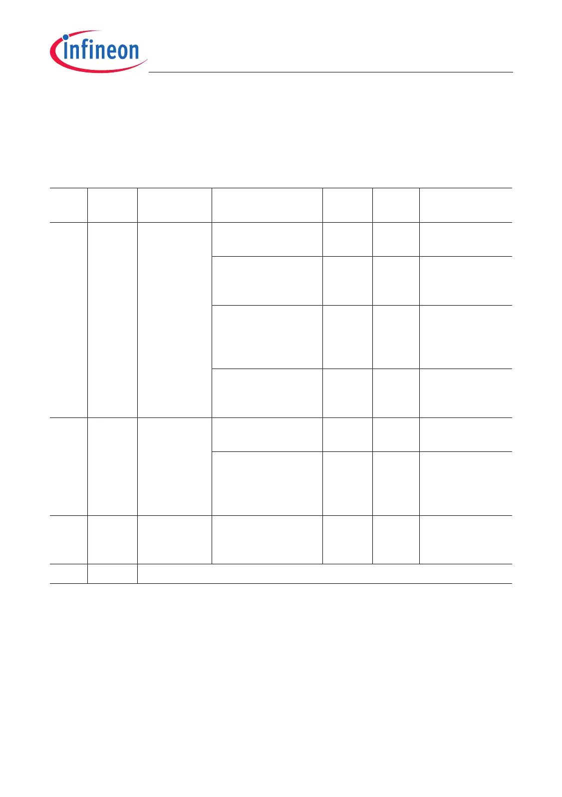
1.4.2 Pad Driver Classes Overview
Table 1-5 gives a overview of the pad driver classes of the TC1796. Further details can
be found in the “TC1796 Data Sheet“.
Table 1-5 Pad Driver and Input Classes Overview
Class Power
Supply
Type Sub Class Speed
Grade
Load Termination
A 3.3 V LVTTL I/O,
LVTTL
outputs
A1
(e.g. GPIO)
6 MHz 100 pF No
A2
(e.g. serial I/Os)
40 MHz 50 pF Series
termination
recommended
A3
(e.g. Trace outputs,
serial I/Os)
75 MHz 50 pF Series
termination
recommended
(for f >25 MHz)
A4
(e.g. Trace Clock)
150
MHz
25 pF Series
termination
recommended
B 2.375 /
3.6 V
1)
1) AC characteristics for EBU pins are valid for 2.5 V ± 5% and 3.3 V ± 5%.
LVTTL
I/O
B1
(e.g. Bus Interface)
40 MHz 50 pF No
B2
(e.g. Bus Clock)
75 MHz 35 pF Series
termination
recommended
(for f >25 MHz)
C 3.3 V LVDS – 50 MHz – Parallel
termination
2)
,
100 Ω ±10%
2) In applications where the LVDS pins are not used (disabled), these pins must be either left unconnected or
properly terminated with the differential parallel termination of 100 Ω ±10%.
D – Analog input, reference voltage inputs.

 Loading...