TC1796
Peripheral Units (Vol. 2 of 2)
General Purpose Timer Array (GPTA)
User’s Manual 24-165 V2.0, 2007-07
GPTA, V2.0
24.3.5 Digital Phase Locked Loop Registers
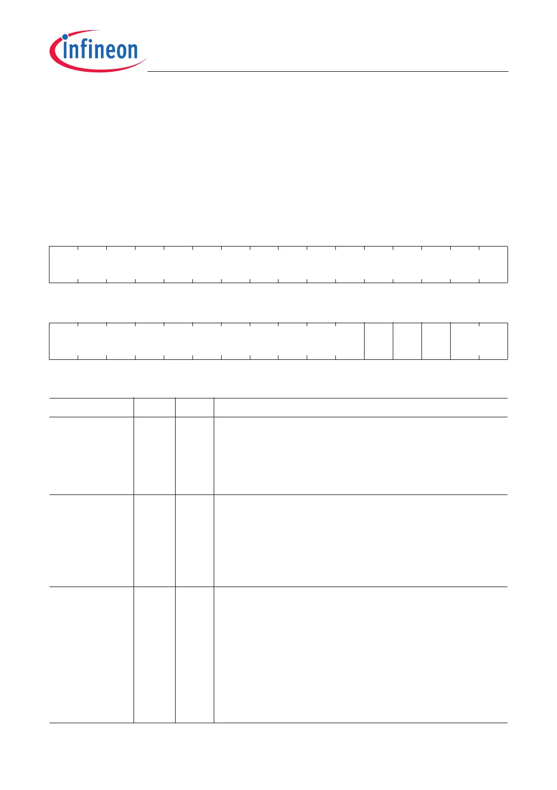
GPTA0_PLLCTR
GPTA0 Phase Locked Loop Control Register
(0C0
H
) Reset Value: 0000 0000
H
GPTA1_PLLCTR
GPTA1 Phase Locked Loop Control Register
(0C0
H
) Reset Value: 0000 0000
H
31 30 29 28 27 26 25 24 23 22 21 20 19 18 17 16
0
r
1514131211109876543210
0 REN PEN AEN MUX
r rw rwh rw rw
Field Bits Type Description
MUX [1:0] rw Trigger Input Channel Selection
00
B
DCM0 output is selected as PLL input
01
B
DCM1 output is selected as PLL input
10
B
DCM2 output is selected as PLL input
11
B
DCM3 output is selected as PLL input
AEN 2rwCompensation of Input Period Length Variation
0
B
Compensation of input signal’s period length
variation is disabled
1
B
Compensation of input signal’s period length
variation (acceleration, deceleration) is
requested
PEN 3rwhUnexpected Period End Behavior
0
B
Counter decrements with constant frequency
1
B
Counter is allowed to decrement with f
GPTA
frequency in case of an input signal period
length’ reduction
Programming PEN to 1 immediately changes the
microtick counter to decrement with f
GPTA
frequency.
This bit is protected during read-modify-write
operations (hardware will win).
 Loading...