TC1796
System Units (Vol. 1 of 2)
General Purpose I/O Ports and Peripheral I/O Lines
User’s Manual 10-12 V2.0, 2007-07
Ports, V2.0
Further details of the temperature compensation logic are described in Section 5.6 on
Page 5-41 (SCU) of this User’s Manual.
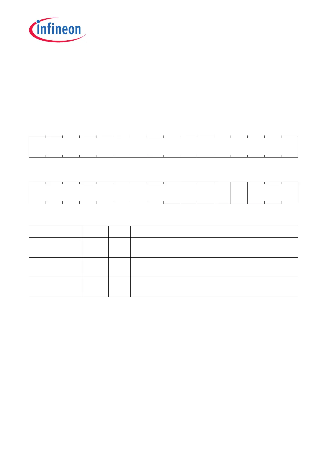
Pad Driver Mode Register Example: Port 0 Pad Driver Mode Register
In addition to the pad driver mode register control selections, a temperature
compensation logic, which is a part of the system control unit (SCU), makes it possible
to adjust the edges of the high-speed class A2 GPIO output lines depending on the die
temperature. The temperature compensation logic affects all class A2 GPIO output lines
that are used simultaneously as output.
The fully programmable temperature compensation logic provides four types of output
driver levels:
• Maximum level (low temperature)
• High level
• Low level
• Minimum level (high temperature)
P0_PDR
Port 0 Pad Driver Mode Register (40
H
) Reset Value: 0000 0000
H
31 30 29 28 27 26 25 24 23 22 21 20 19 18 17 16
0
r
1514131211109876543210
0 PD10PD0
rrwrrw
Field Bits Type Description
PD0 [2:0] rw Pad Driver Mode for P0.[7:0]
(Class A1 pads; coding see Page 10-11)
PD1 [6:4] rw Pad Driver Mode for P0.[15:8]
(Class A1 pads; coding see Page 10-11)
0 3,
[31:7]
r Reserved
Read as 0; should be written with 0.

 Loading...