TC1796
Peripheral Units (Vol. 2 of 2)
Synchronous Serial Interface (SSC)
User’s Manual 20-50 V2.0, 2007-07
SSC, V2.1
Clock Control Register
The Clock Control Registers SSC0_CLC and SSC0_CLC make it possible to control
(enable/disable) the clock signals f
CLC0
and f
CLC1
under certain conditions. Each SSC has
its own clock control register.
Note: After a hardware reset operation, the f
CLCx
clocks are disabled, and therefore also
the SSC modules are disabled (DISS set).
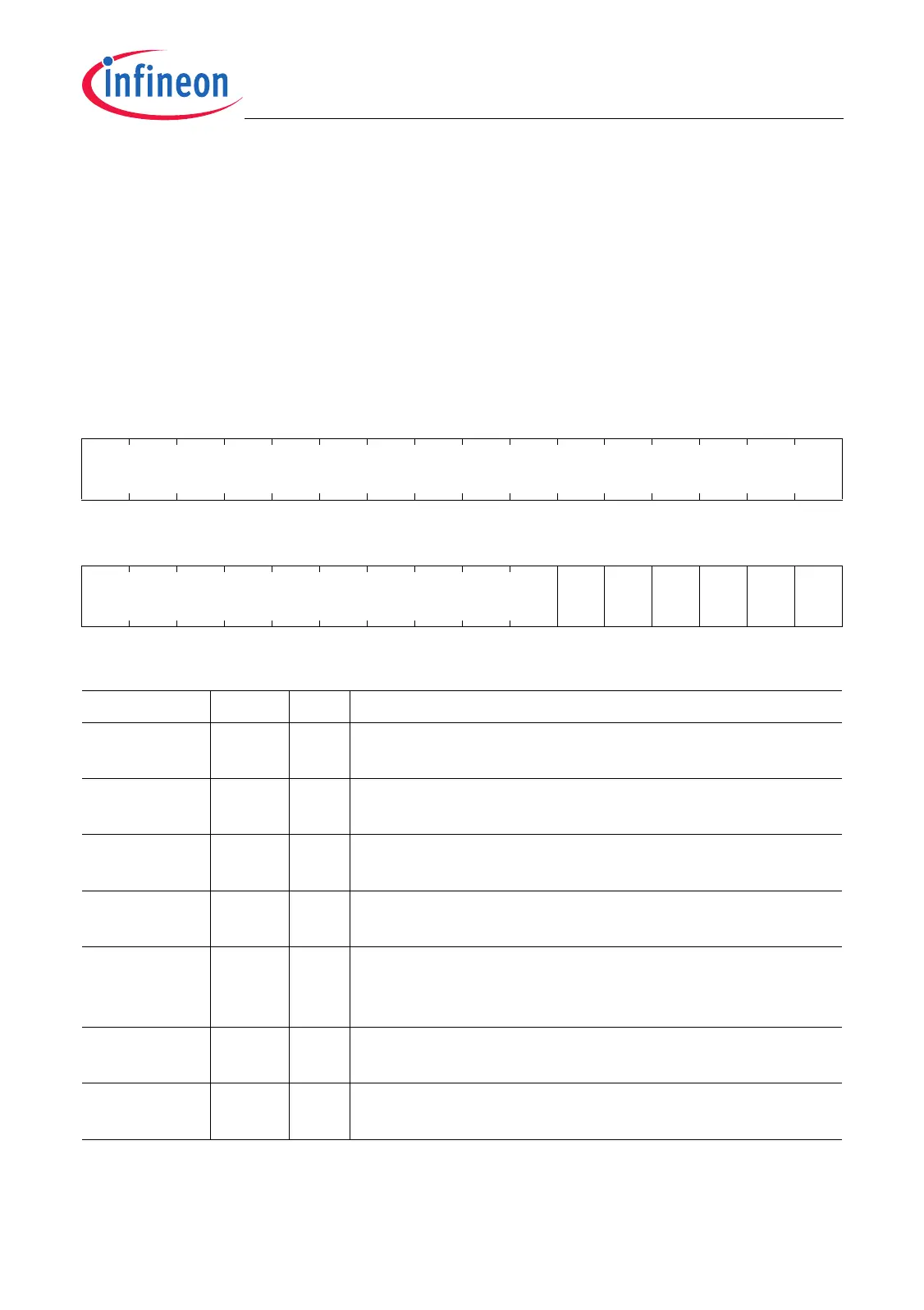
SSC0_CLC
SSC0_Clock Control Register (00
H
) Reset Value: 0000 0003
H
SSC1_CLC
SSC1 Clock Control Register (00
H
) Reset Value: 0000 0003
H
31 30 29 28 27 26 25 24 23 22 21 20 19 18 17 16
0
r
1514131211109876543210
0
FS
OE
SB
WE
E
DIS
SP
EN
DIS
S
DIS
R
rrwwrwrwrrw
Field Bits Type Description
DISR 0rwModule Disable Request Bit
Used for enable/disable control of the module.
DISS 1rModule Disable Status Bit
Bit indicates the current status of the module.
SPEN 2rwModule Suspend Enable for OCDS
Used to enable the suspend mode.
EDIS 3rwExternal Request Disable
Used to control the external clock disable request.
SBWE 4wModule Suspend Bit Write Enable for OCDS
Determines whether SPEN and FSOE are write-
protected.
FSOE 5rwFast Switch Off Enable
Used for fast clock switch off in suspend mode.
0 [31:6] r Reserved
Read as 0; should be written with 0.

 Loading...