TC1796
Peripheral Units (Vol. 2 of 2)
Micro Second Channel (MSC)
User’s Manual 21-60 V2.0, 2007-07
MSC, V2.0
The four Upstream Data Registers UDx store the content (data, addresses, received and
calculated parity bit, parity error bit) of a received upstream channel data frame.
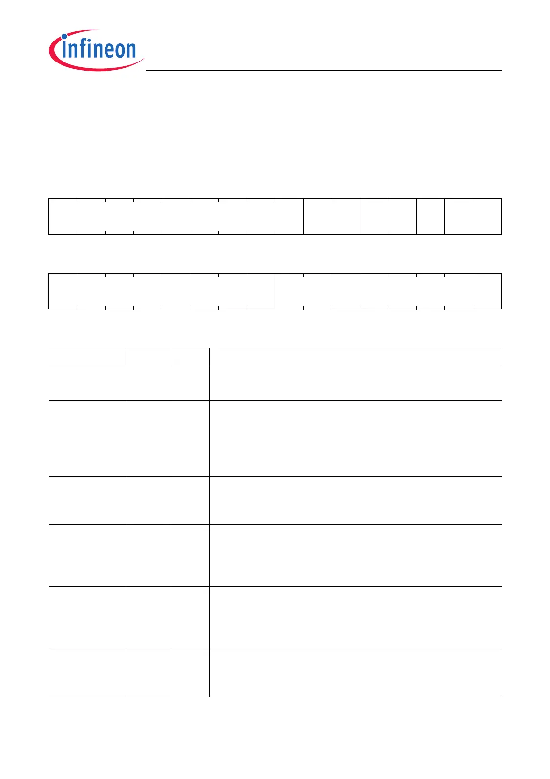
UDx (x = 0-3)
Upstream Data Register x (30
H
+x*4
H
) Reset Value: 0000 0000
H
31 30 29 28 27 26 25 24 23 22 21 20 19 18 17 16
0
P
ERR
IPF LABF C P V
r rh rh rh w rh rh
1514131211109876543210
0DATA
rrh
Field Bits Type Description
DATA [7:0] rh Received Data
This bit field contains the 8-bit receive data.
V 16 rh Valid Bit
This bit is set by hardware when the received data is
written to UDx. Writing bit C = 1 clears V. If hardware
setting and software clearing of the valid bit occur
simultaneously, bit V will be cleared.
P 17 rh Parity Bit
This flag contains the parity bit that has been received
with the data frame.
C 18 w Clear Bit
0
B
No operation.
1
B
Bit V is cleared.
Bit C is always read as 0.
LABF [20:19] rh Lower Address Bit Field
This bit field contains the two address bits A[1:0] of the
4-bit address field (16-bit data frame). If 12-bit data
frame is selected, LABF is always set to 00
B
.
IPF 21 rh Internal Parity Flag
This bit contains the parity bit that has been calculated
in the MSC during data frame reception.

 Loading...