TC1796
System Units (Vol. 1 of 2)
Clock System and Control
User’s Manual 3-31 V2.0, 2007-07
Clock, V2.0
Note: In the TC1796, the fractional divider input clock f
IN
is also referred to as f
CLC
and
the fractional divider input clock f
OUT
is also referred to as f
MOD
(see Figure 3-5).
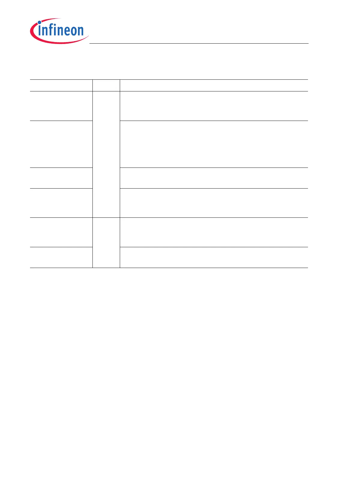
Table 3-7 Fractional Divider Control I/O Lines
Signal I/O Description
Debug Suspend
Request
Input This input becomes active when a general suspend
request is issued from the debug system to the on-chip
modules.
Debug Suspend
Acknowledge
This input is driven with the disable acknowledge signal
from the module kernel. This disable acknowledge signal
is activated by the module kernel as a response to a
suspend request that has been generated by the fractional
divider via the Kernel Disable Request signal.
External Clock
Enable
This input can be used to synchronize the fractional
divider clock generation to external events.
Module Disable
Request
This input is connected to the disable request output from
the CLC logic (see Figure 3-5). An active signal at this
input activates the Kernel Disable Request signal.
Kernel Disable
Request
Output This output signal becomes active when either the Module
Disable Request input or the Debug Suspend Request
input become active.
Reset External
Divider
This output signal makes it possible to control (stop/reset)
external divider stages which have f
OUT
as input.

 Loading...