TC1796
Peripheral Units (Vol. 2 of 2)
General Purpose Timer Array (GPTA)
User’s Manual 24-196 V2.0, 2007-07
GPTA, V2.0
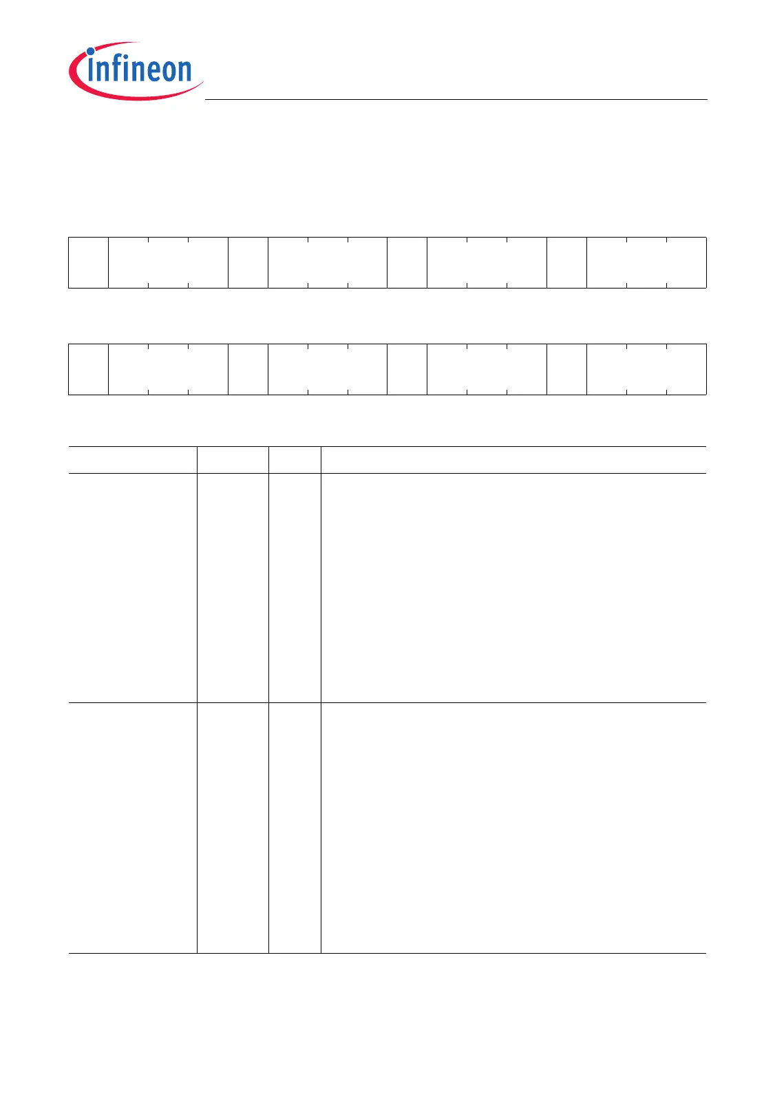
OMCRHg (g = 0-13)
Output Multiplexer Control Register for Upper Half of Output Group g
Reset Value: 0000 0000
H
31 30 29 28 27 26 25 24 23 22 21 20 19 18 17 16
0OMG70OML70OMG60OML6
rrwrrwrrwrrw
1514131211109876543210
0OMG50OML50OMG40OML4
rrwrrwrrwrrw
Field Bits Type Description
OML4,
OML5,
OML6,
OML7
[2:0],
[10:8],
[18:16],
[26:24]
rw Multiplexer Line Selection
This bit field selects the input line of a OMG that can
be selected by bit field OMGn for OMG output n.
000
B
OMG input IN0 selected
001
B
OMG input IN1 selected
010
B
OMG input IN2 selected
011
B
OMG input IN3 selected
100
B
OMG input IN4 selected
101
B
OMG input IN5 selected
110
B
OMG input IN6 selected
111
B
OMG input IN7 selected
OMG4,
OMG5,
OMG6,
OMG7
[6:4],
[14:12],
[22:20],
[30:28]
rw Multiplexer Group Selection
This bit field determines the OMGng which is
connected to input n of I/O Group g or Output group
g-7.
X00
B
OMG0g selected
X0X
B
OMG1g selected
X10
B
OMG2g selected
All other combinations are reserved. If a reserved
combination of OMGn value is selected, the
corresponding OMG output is forced to 0 level. For
compatibility reasons, OMGn[2] = 0 should be used
(as value for X) for OMGn bit field programming.

 Loading...