TC1796
System Units (Vol. 1 of 2)
System Control Unit
User’s Manual 5-42 V2.0, 2007-07
SCU, V2.0
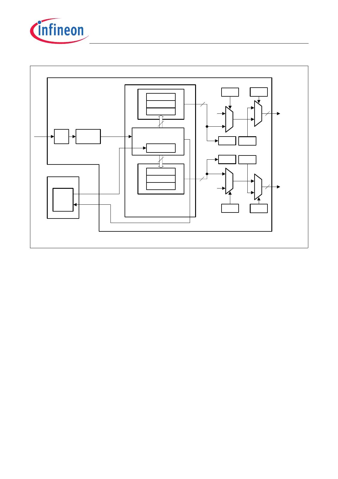
Figure 5-8 Pad Driver Temperature Compensation Block Diagram
Generally, temperature compensation is a transparent feature. Bit field
SCU_TCLRx.THCOUNT (x = 0, 1) of both temperature compensation x level registers
provides direct access to the actual compensation (counter) value and allows software
adjustment control of the port temperature compensation logic. This is useful for two
situations:
1. Device testing: The function of the compensation mechanism can be verified during
production testing or characterization.
2. User control: During operation the device can be controlled via externally provided
compensation values rather than via the internal mechanism.
Temperature compensation is initialized by programming register SCU_TCCON (enable
and prescaler for 100 kHz reference clock) and register SCU_TCLR0 and SCU_TCLR1
(levels values).
The temperature-dependent counter value THCOUNT is compared against three
thresholds values (correspond to a certain temperature level) at which the 2-bit output
signals to the pad logic are switched (see Figure 5-9). The three threshold values are
defined by three bit fields in the port temperature compensation 0/1 level registers
SCU_TCLR0 and SCU_TCLR1. The pads support different driving levels and are
controlled via the 2-bit output signals.
MCB05619
100 KHz
THMAX1
THMED1
THMIN1
M
U
X
1/TCDIV
f
REF
f
SYS
4:1
M
U
X
2
To Pad
Logic of
Class A2
GPIO
Outputs
THCOUNT
M
U
X
M
U
X
To Pad
Logic of
EBU
Outputs
TCS1
TCE1
11
B
Temperature
Compensation
Control
THMIN0
THMED0
THMAX0
OSC
Pad
8
Control
f
POSC
System
Control
Unit
TCC1
TCV1
TCC0
TCV0
11
B
TCS0
TCE0
Enable
POSCEN
2
2
2
8
 Loading...