TC1796
System Units (Vol. 1 of 2)
Peripheral Control Processor (PCP)
User’s Manual 11-27 V2.0, 2007-07
PCP, V2.0
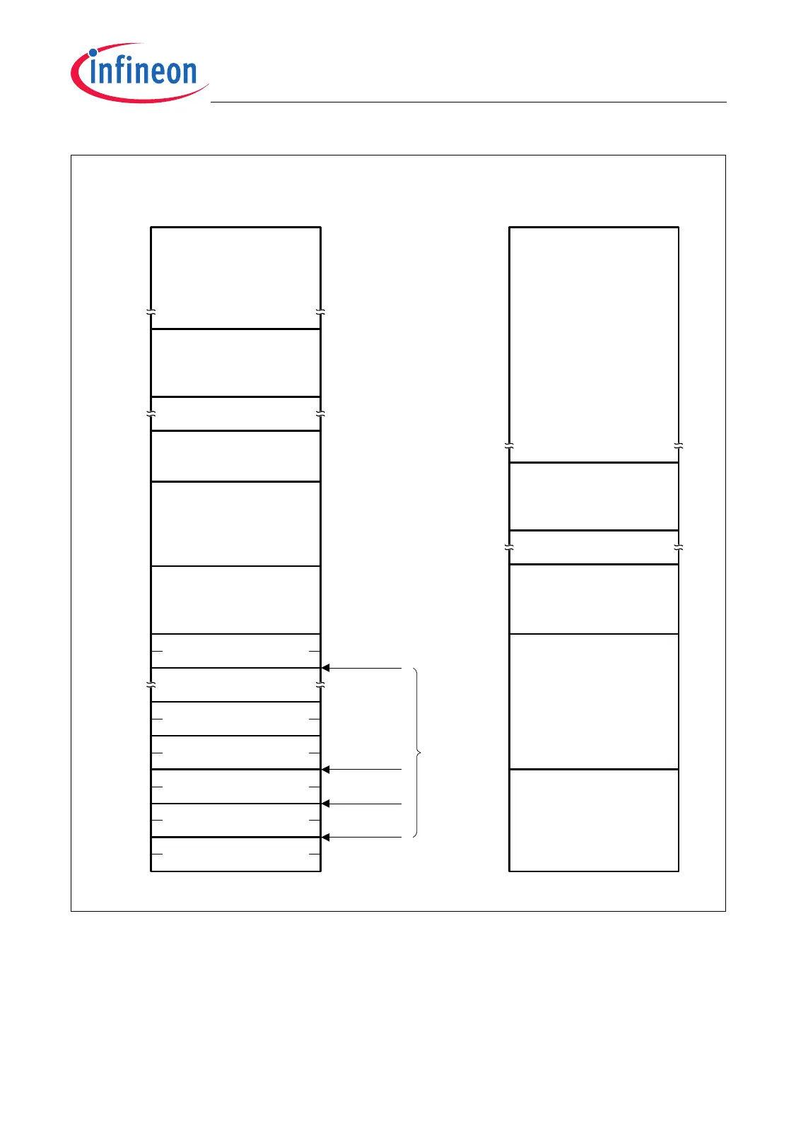
Figure 11-10 Examples of Code Memory Organization for Channel Restart and
Channel Resume Modes
Note: The CMEM address offsets in the above figure are shown as PCP instruction (half-
word) offsets. To obtain FPI address offsets (byte offset), multiply each offset by
two.
Code Memory
CMEM
Instruction #1
2 Half-words
not used
Instruction #2
MCA05675
00
H
02
H
SRPN = 1
Channel
#1
04
H
Instruction #2
Instruction #1
Channel
#2
SRPN = 2
SRPN = 3
06
H
Instruction #2
Instruction #1
Channel
#3
SRPN = n1
n1×2
H
Instruction #1
Instruction #2
Channel
#1
Channel #1
Main Code
Channel #3
Main Code
Channel #n1
Main Code
Channel #2
Main Code
Channel Restart Mode
16 0
Channel
Entry
Table
Channel Resume Mode
16 0
Channel #1
Main Code
00
H
Channel #3
Main Code
Channel #n1
Main Code
Channel #2
Main Code
Code Memory
CMEM

 Loading...