TC1796
System Units (Vol. 1 of 2)
Introduction
User’s Manual 1-47 V2.0, 2007-07
Intro, V2.0
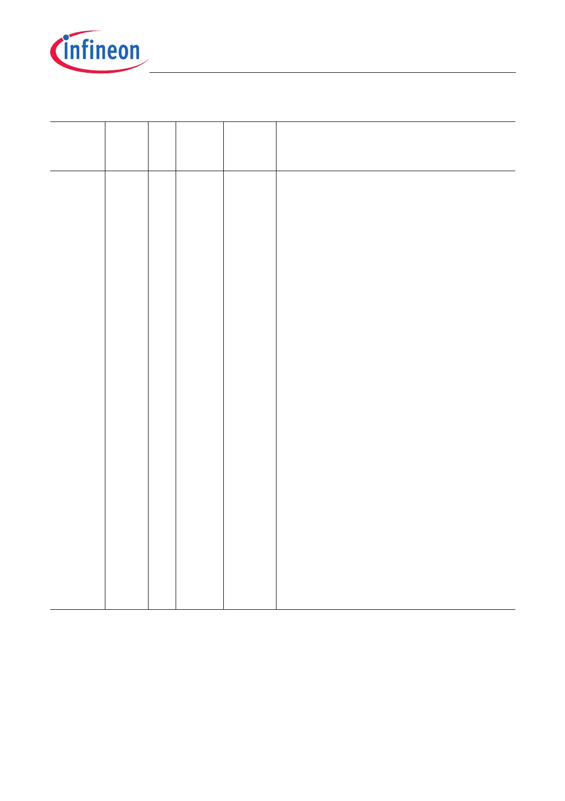
P8 I/O A1/A2 V
DDP
Port 8
Port 8 is an 8-bit bi-directional general-
purpose I/O port which can be alternatively
used for the MLI1 interface or as GPTA I/O
lines.
P8.0
P8.1
P8.2
P8.3
P8.4
P8.5
P8.6
P8.7
H2
H1
J3
J2
J1
K2
K3
K1
O
I/O
I
I/O
O
I/O
O
I/O
I
I/O
O
I/O
I
I/O
I
I/O
A2
A2
A1
A1
A2
A2
A2
A2
A1
A1
A2
A2
A1
A1
A1
A1
TCLK1
IN40 / OUT40
TREADY1A
IN41 / OUT41
TVALID1A
IN42 / OUT42
TDATA1
IN43 / OUT43
RCLK1A
IN44 / OUT44
RREADY1A
IN45 / OUT45
RVALID1A
IN46 / OUT46
RDATA1A
IN47 / OUT47
MLI1 transmit channel clock
output
line of GPTA
MLI1 transmit channel
ready input A
line of GPTA
MLI1 transmit channel valid
output A
line of GPTA
MLI1 transmit channel data
output A
line of GPTA
MLI1 receive channel clock
input A
line of GPTA
MLI1 receive channel ready
output A
line of GPTA
MLI1 receive channel valid
input A
line of GPTA
MLI1 receive channel data
input A
line of GPTA
Table 1-3 Pin Definitions and Functions (cont’d)
Symbol Pins I/O Pad
Driver
Class
Power
Supply
Functions
 Loading...