TC1796
Peripheral Units (Vol. 2 of 2)
Asynchronous/Synchronous Serial Interface (ASC)
User’s Manual 19-39 V2.0, 2007-07
ASC, V2.0
Pad Driver Mode Registers
The Port 5 and Port 6 pad driver mode register contains bit fields that determine the
output driver strength and the slew rate of ASC output lines.
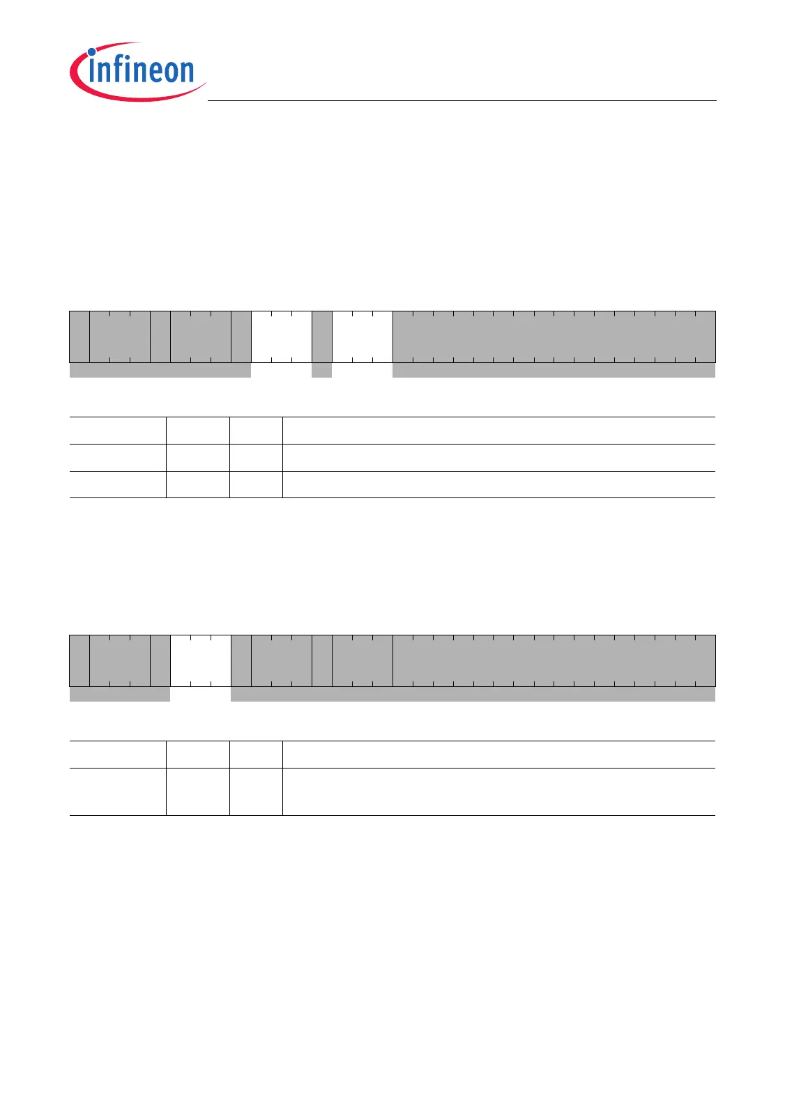
P5_PDR
Port 5 Pad Driver Mode Register (40
H
) Reset Value: 0000 0000
H
31 22 20 18 16 0
0
PD
MSC1
0
PD
MSC0
0
PD
ASC1
0
PD
ASC0
0
r rw r rw rrwrrw r
Field Bits Type Description
PDASC0 [18:16] rw Pad Driver Mode for P5.0/RXD0A and P5.1/TXD0A
1)
1) Coding of bit field see Table 19-10. Shaded bits and bit fields are “don’t care” for ASC I/O port control.
PDASC1 [22:20] rw Pad Driver Mode for P5.2/RXD1A and P5.3/TXD1A
1)
P6_PDR
Port 6 Pad Driver Mode Register (40
H
) Reset Value: 0000 0000
H
31 26 24 0
0
PD
CAN23
0
PD
CAN01
0
PD
SSC1
0
PD
SSC0
0
r rw rrwr rw r rw r
Field Bits Type Description
PDCAN01 [26:24] rw Pad Driver Mode for P6.8/RXD0B, P6.9/TXD0B,
P6.10/RXD1B, and P6.11/TXD1B
1)
1) Coding of bit field see Table 19-10. Shaded bits and bit fields are “don’t care” for ASC I/O port control.

 Loading...