TC1796
Peripheral Units (Vol. 2 of 2)
Analog-to-Digital Converter (ADC)
User’s Manual 25-2 V2.0, 2007-07
ADC, V2.0
• Programmable sample and conversion timing schemes
• Limit checking
• Flexible ADC module service request control unit
• Synchronization of the two on-chip A/D Converters
• Automatic control of external analog multiplexers
• Equidistant samples initiated by timer
• External trigger and gating inputs for conversion requests
• Power reduction and clock control feature
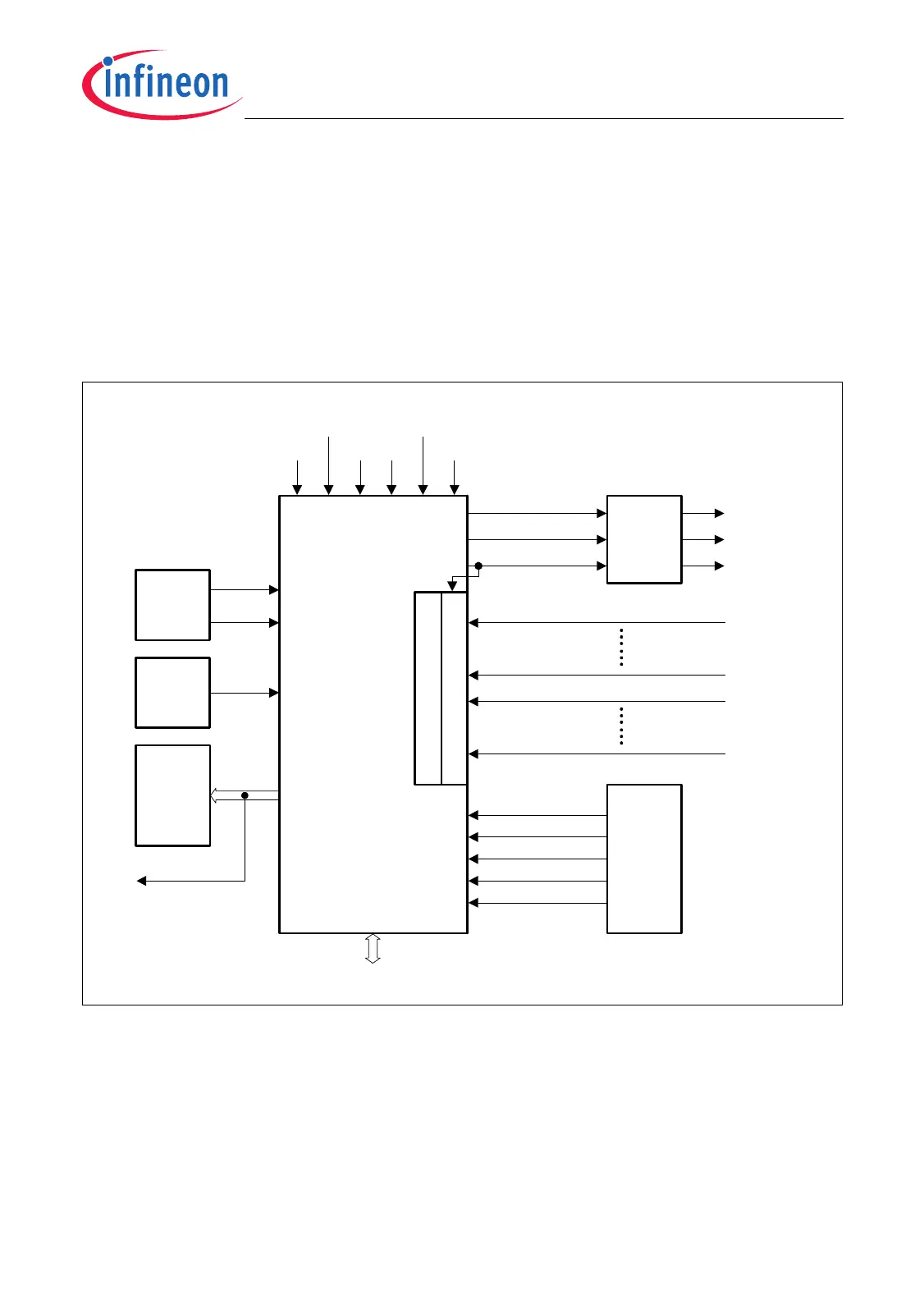
Figure 25-1 General Block Diagram of the ADC Module
As shown in Figure 25-1, each of the two ADC modules, ADC0 and ADC1 has 16 analog
input channels. An analog multiplexer selects the input line for the analog input channels
from among 32 analog inputs. Additionally, an external analog multiplexer can be used
for analog input extension. External Clock control, address decoding, and service
request (interrupt) control are managed outside the ADC module kernel. A
synchronization bridge is used for synchronization of two ADC modules. External trigger
Interrupt
Control
Clock
Control
Address
Decoder
ADC
Module
Kernel
f
ADC
SR[7:0]
Port
Control
MCB06004
Synchronization Bridge
V
AGND
V
DD
V
SS
V
DDM
V
AREF
V
SSM
Group 1
f
CLC
Group 0
External
Request
Unit
ASGT
SW0TR, SW0GT
ETR, EGT
QTR, QGT
TTR, TGT
EMUX0
EMUX1
GRPS
To DMA
Analog Input Multiplexer
16 Analog Input Channels
EMUX0
EMUX1
GRPS
AIN0
AIN15
AIN16
AIN31

 Loading...