TC1796
Peripheral Units (Vol. 2 of 2)
Fast Analog-to-Digital Converter (FADC)
User’s Manual 26-55 V2.0, 2007-07
FADC, V2.0
The Final Result Registers for filters 0 and 1 hold the final result of the filter operations.
Note: During a final result calculation phase (phase C in Figure 26-8 on Page 26-16),
the contents of the FRRn registers change. Therefore, it is recommended to read
a final result from the FRRn registers immediately (for example, by a DMA
operation) after a corresponding interrupt request flag CRSR.IRQFn has been set.
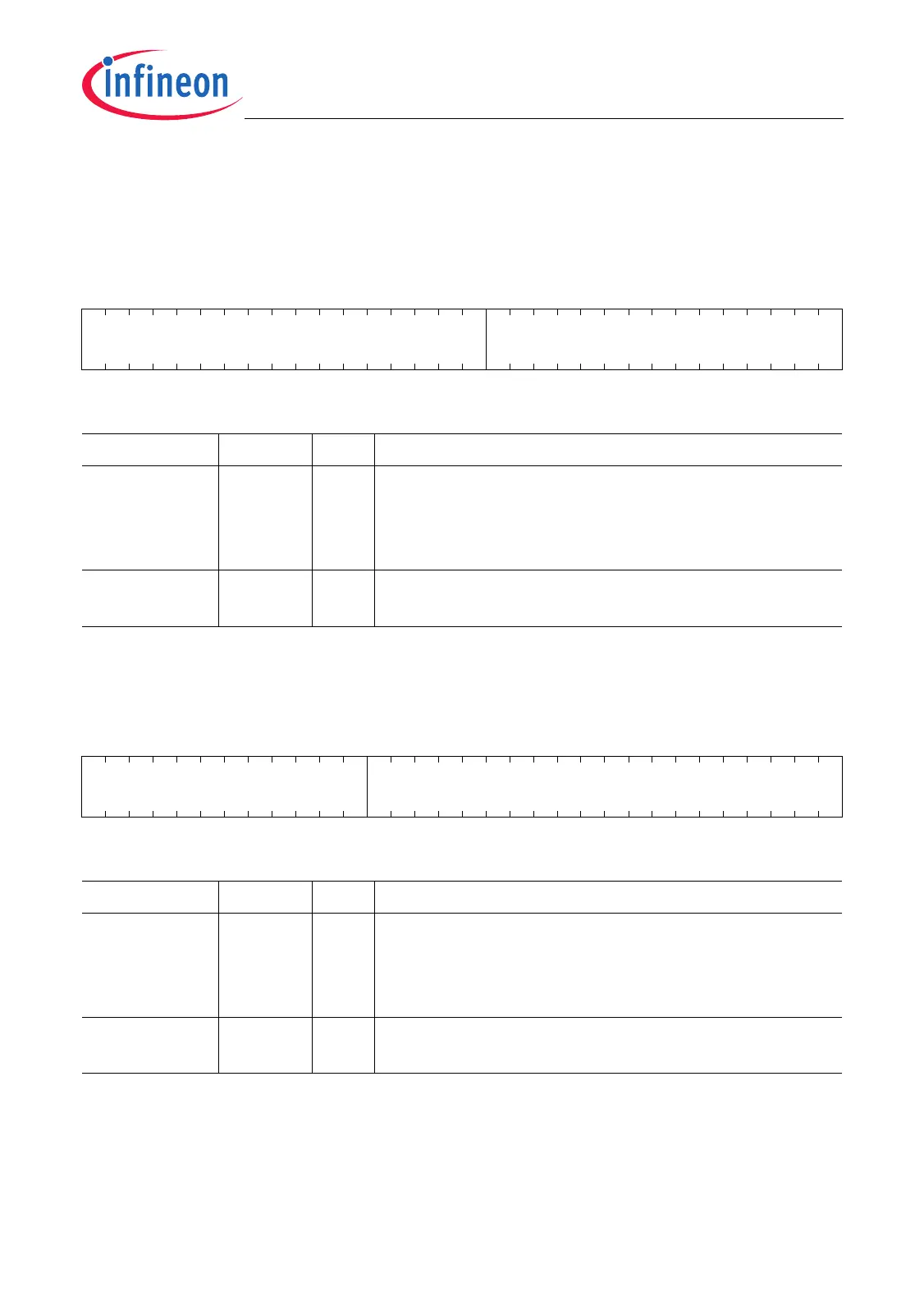
FRR0
Filter 0 Final Result Register (74
H
) Reset Value: 0000 0000
H
31 15 14 0
0FR
rrh
Field Bits Type Description
FR [14:0] rh Final Result
This bit field contains the right-aligned 15-bit final
result of filter 0.
FR is cleared when writing GCR.RSTFn = 1.
0 [31:15] r Reserved
Read as 0.
FRR1
Filter 1 Final Result Register (94
H
) Reset Value: 0000 0000
H
31 20 19 0
0FR
rrh
Field Bits Type Description
FR [19:0] rh Final Result
This bit field contains the right-aligned 20-bit final
result of filter 1.
FR is cleared when writing GCR.RSTFn = 1.
0 [31:20] r Reserved
Read as 0.

 Loading...