TC1796
System Units (Vol. 1 of 2)
Reset and Boot Operation
User’s Manual 4-30 V2.0, 2007-07
Reset, V2.0
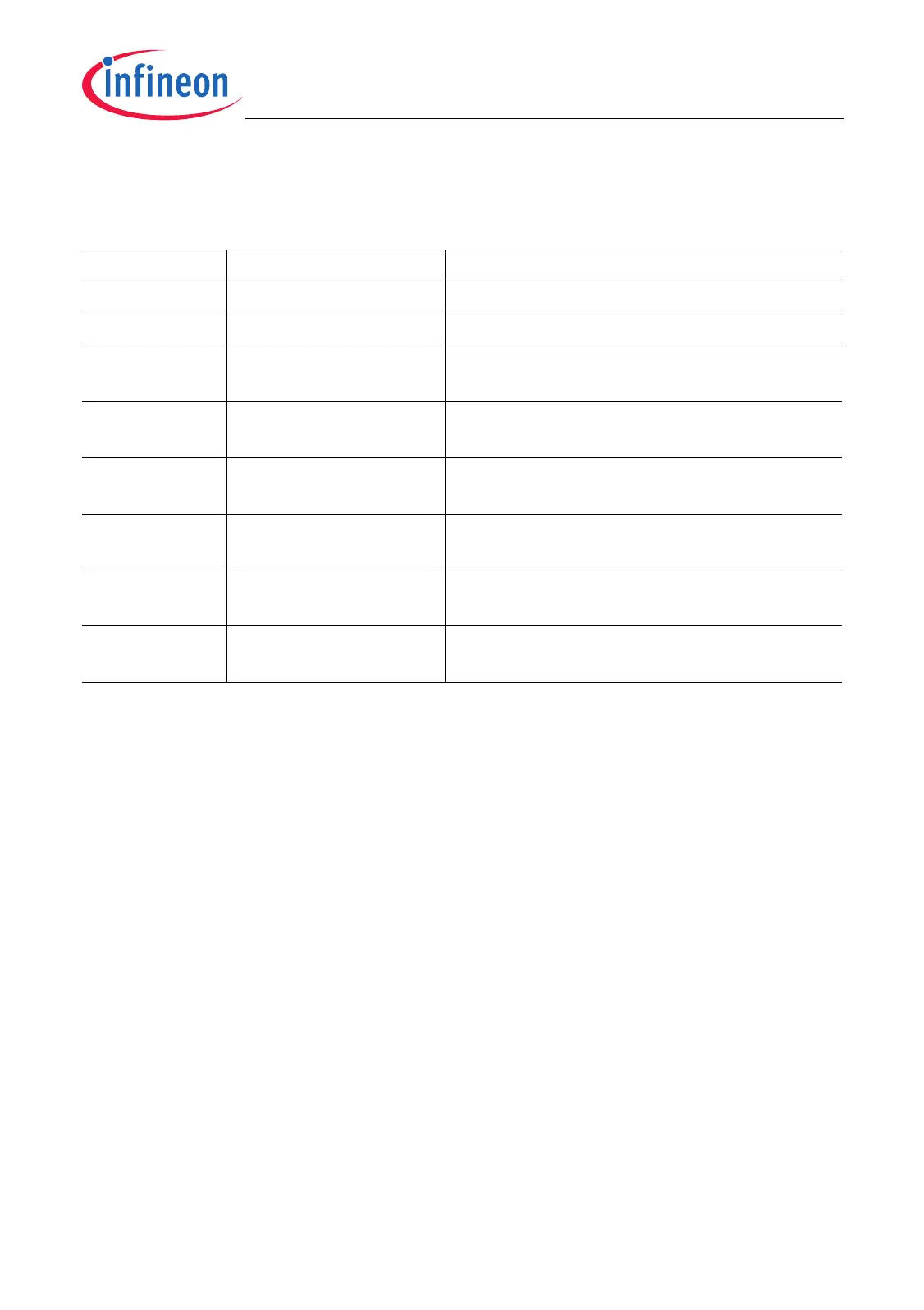
Table 4-9 shows the structure of the ABM headers.
The time needed for CRC generation depends on the length of the memory range to be
checked. In case of internal PFLASH check, the duration can be roughly calculated as
follows:
• CRC of header: To be defined
• CRC of a Flash space of 400 bytes: To be defined
Table 4-9 Structure of ABM Headers
Address
1)
1) XXXX XX is 8001 FF
H
/A001 FF
H
for primary ABM header and 8003 FF
H
/A003 FF
H
for secondary ABM header
(see also Table 4-8).
Value Function
XXXX XXE0
H
32-bit start address Program/code start address
XXXX XXE4
H
DEAD BEEF
H
Identifier string
XXXX XXE8
H
32-bit address
(checksum start)
32-bit aligned start address of memory
range to be checked
XXXX XXEC
H
32-bit address
(checksum end)
32-bit aligned end address (last word
address) of memory range to be checked
XXXX XXF0
H
32-bit CRC value
CRC
RANGE
Expected 32-bit CRC result for memory
range to be checked
XXXX XXF4
H
CRC
RANGE
inverted Inverted expected 32-bit CRC result for
memory range to be checked
XXXX XXF8
H
32-bit CRC value
CRC
HEAD
CRC result of current ABM header from
offset (byte) address E0
H
to F7
H
XXXX XXFC
H
CRC
HEAD
inverted Inverted CRC result of current ABM header
from offset (byte) address E0
H
to F7
H

 Loading...