TC1796
System Units (Vol. 1 of 2)
Data Memory Unit
User’s Manual 8-4 V2.0, 2007-07
DMU, V2.0
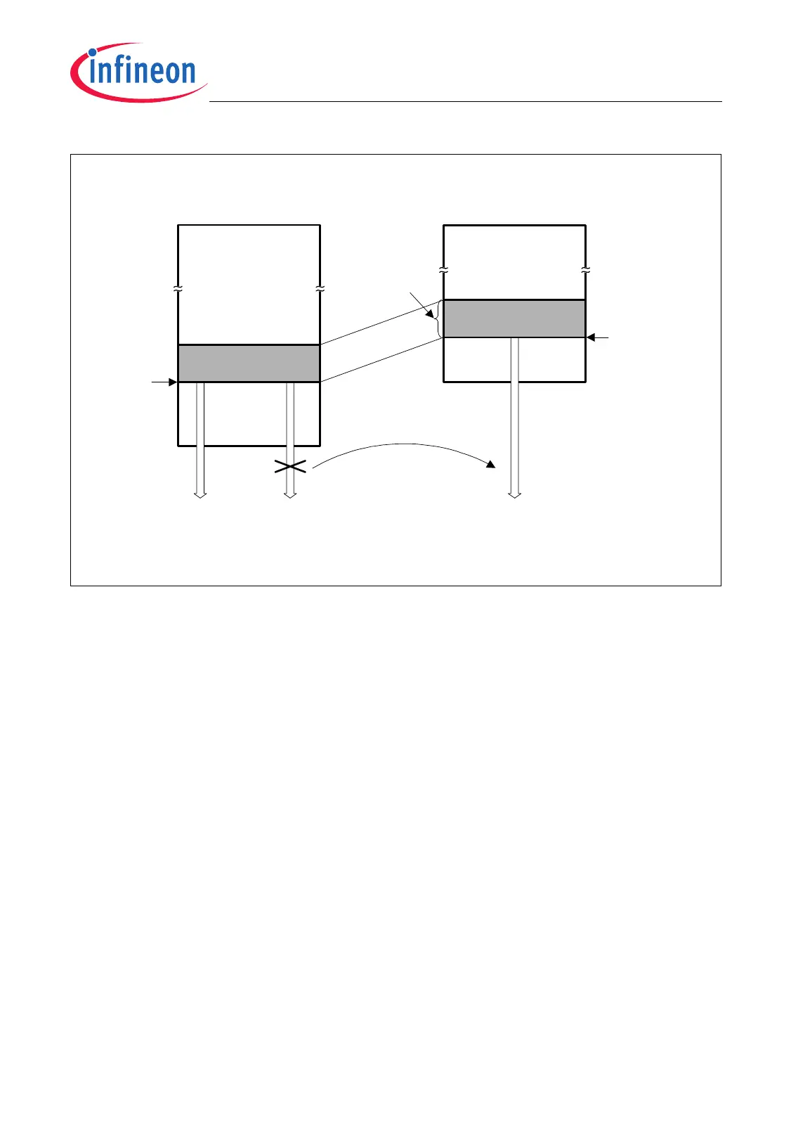
Figure 8-2 Redirection of Data Read Accesses from Code Memory to Internal
Data Memory
In the TC1796, the complete 64 Kbyte SRAM of the DMU can be used as overlay
memory. Sixteen overlay memory blocks within the SRAM with programmable base
address and block sizes are supported, and can be individually enabled for overlay
functionality. The block size of each overlay memory block can be in the range of 2 bytes
up to 512 bytes.
Attention: In the TC1796ED emulation device, it is possible in addition to redirect
code memory data accesses to the emulation memory of the
TC1796ED.
Code
Fetch
(unaffected)
MCA05649
Data
Read/ Write
Redirect
Target
Address
(OTARx)
Internal or External
Code Memory
Overlay Target
Code Memory
DMU Memory
Overlay
Memory Block x
Base Address
(RABRx)
Block Size
(OMASKx)
Data
Read/ Write

 Loading...