TC1796
System Units (Vol. 1 of 2)
Direct Memory Access Controller
User’s Manual 12-87 V2.0, 2007-07
DMA, V2.0
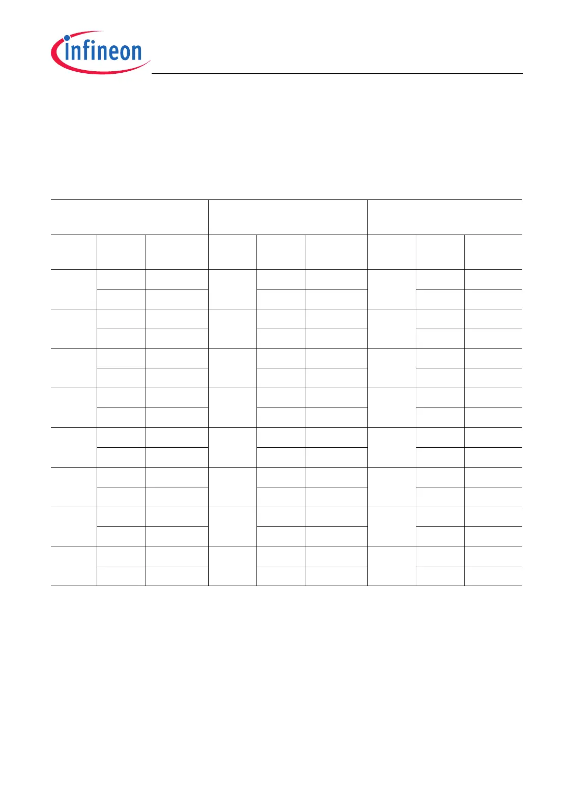
Table 12-8 shows the offset values that are added or subtracted to/from a source or
destination address register after a DMA move. Bit field SMF and bit INCS determine the
offset value for the source address. Bit field DMF and bit INCD determine the offset value
for the destination address.
Note: CHCRmx.CHDW = 11
B
is reserved and should not be used.
Table 12-8 Address Offset Calculation Table
CHCRmx.CHDW = 00
B
(8-bit Data Width)
CHCRmx.CHDW = 01
B
(16-bit Data Width)
CHCRmx.CHDW = 10
B
(32-bit Data Width)
SMF
DMF
INCS
INCD
Address
Offset
SMF
DMF
INCS
INCD
Address
Offset
SMF
DMF
INCS
INCD
Address
Offset
000
B
0 -1 000
B
0-2 000
B
0-4
1+1 1+2 1+4
001
B
0 -2 001
B
0-4 001
B
0-8
1+2 1+4 1+8
010
B
0 -4 010
B
0-8 010
B
0-16
1+4 1+8 1+16
011
B
0 -8 011
B
0 -16 011
B
0-32
1 +8 1 +16 1 +32
100
B
0 -16 100
B
0 -32 100
B
0-64
1 +16 1 +32 1 +64
101
B
0 -32 101
B
0 -64 101
B
0-128
1 +32 1 +64 1 +128
110
B
0 -64 110
B
0-128110
B
0-256
1 +64 1 +128 1 +256
111
B
0 -128 111
B
0-256111
B
0-512
1 +128 1 +256 1 +512

 Loading...