TC1796
System Units (Vol. 1 of 2)
Introduction
User’s Manual 1-53 V2.0, 2007-07
Intro, V2.0
System I/O
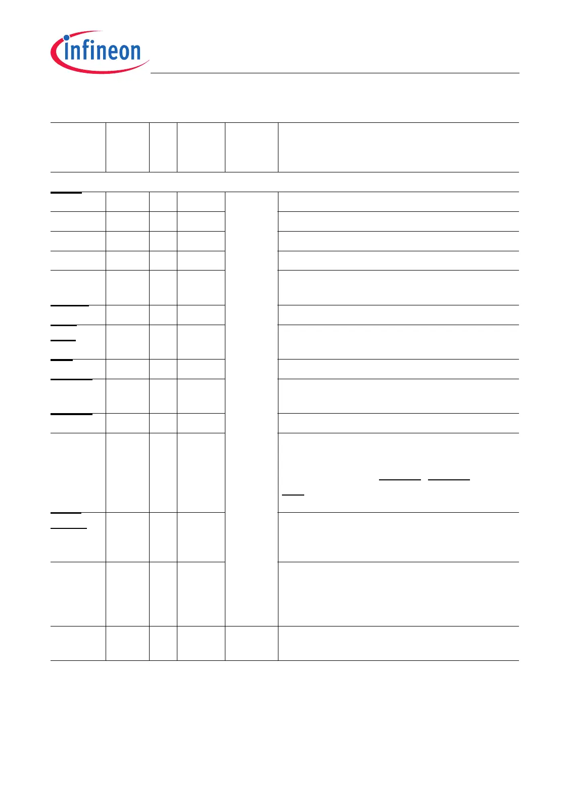
TRST F23 I A2 V
DDP
JTAG Module Reset/Enable Input
3)
TCK E24 I A2 JTAG Module Clock Input
3)
TDI E25 I A1 JTAG Module Serial Data Input
TDO D25 O A2 JTAG Module Serial Data Output
TMS F24 I A1 JTAG Module State Machine Control
Input
BRKIN C26 I/O A3 OCDS Break Input (Alternate Output)
3)
BRK
OUT
D26 I/O A3 OCDS Break Output (Alternate Input
3)
NMI A22 I –
4)
Non-Maskable Interrupt Input
HDRST A23 I/O A2
5)
Hardware Reset Input/
Reset Indication Output
PORST B22 I –
4)
Power-on Reset Input
BYPASS A24 I – PLL Bypass Select Input
This input has to be held stable between
two power-on resets. With BYPASS = 1 the
spike filters in the HDRST, PORST, and
NMI inputs are switched off.
TEST
MODE
B23 I –
6)
Test Mode Select Input
For normal operation of the TC1796, this pin
should be connected to high level.
TSTRES G24 I –
6)
Test Reset Input
For normal operation of the TC1796, this pin
must be connected to low level. Otherwise
an unpredictable reset behavior may occur.
XTAL1
XTAL2
G26
G25
I
O
n.a. V
DD
Oscillator / PLL / Clock Generator Input /
Output Pins
3)
Table 1-3 Pin Definitions and Functions (cont’d)
Symbol Pins I/O Pad
Driver
Class
Power
Supply
Functions

 Loading...