www.ti.com
Message RAM
1431
SPNU563A–March 2018
Submit Documentation Feedback
Copyright © 2018, Texas Instruments Incorporated
Controller Area Network (DCAN) Module
27.5.3 Message RAM Representation in Debug/Suspend Mode
In Debug/Suspend mode, the Message RAM will be memory mapped. This allows the external debug unit
to access the Message RAM.
NOTE: During Debug/Suspend Mode, the Message RAM cannot be accessed via the IFx register
sets.
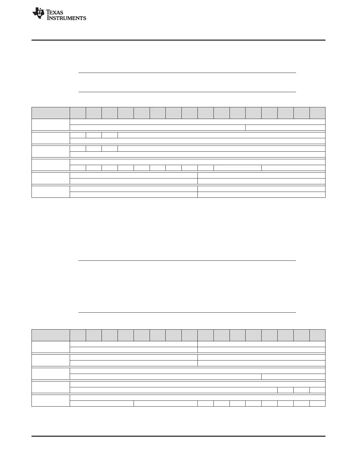
Figure 27-5. Message RAM Representation in Debug/Suspend Mode
Bit 31 30 29 28 27 26 25 24 23 22 21 20 19 18 17 16
15 14 13 12 11 10 9 8 7 6 5 4 3 2 1 0
MsgAddr + 0x00
Reserved
Reserved Reserved
MsgAddr + 0x04
MXtd MDir Rsvd Msk[28:16]
Msk[15:0]
MsgAddr + 0x08
Rsvd Xtd Dir ID[28:16]
ID[15:0]
MsgAddr + 0x0C
Reserved
Rsvd MsgLst Rsvd UMask TxIE RxIE RmtEn Rsvd EOB Reserved DLC[3:0]
MsgAddr + 0x10
Data 3 Data 2
Data 1 Data 0
MsgAddr + 0x14
Data 7 Data 6
Data 5 Data 4
27.5.4 Message RAM Representation in Direct Access Mode
When the RDA bit in Test Register is set while the DCAN module is in Test Mode (Test bit in CAN control
register is set), the CPU has direct access to the Message RAM. Due to the 32-bit bus structure, the RAM
is split into word lines to support this feature. The CPU has access to one word line at a time only.
In RAM Direct Access mode, the RAM is represented by a continuous memory space within the address
frame of the DCAN module, starting at the Message RAM base address.
NOTE: During Direct Access Mode, the Message RAM cannot be accessed via the IFx register sets.
Before entering RDA mode, it must be ensured that the Init bit is set to avoid any conflicts
with the message handler accessing the message RAM.
Any read or write to the RAM addresses for RamDirectAccess during normal operation mode
(TestMode bit or RDA bit is not set) will be ignored.
Writes to Reserved bits have no effect.
Figure 27-6. Message RAM Representation in RAM Direct Access Mode
Bit 31 30 29 28 27 26 25 24 23 22 21 20 19 18 17 16
15 14 13 12 11 10 9 8 7 6 5 4 3 2 1 0
MsgAddr + 0x00
Data 4 Data 5
Data 6 Data 7
MsgAddr + 0x04
Data 0 Data 1
Data 2 Data 3
MsgAddr + 0x08
ID[27:12]
ID[11:0] DLC[3:0]
MsgAddr + 0x0C
Msk[28:13]
Msk[12:0] Xtd Dir ID[28]
MsgAddr + 0x10
Reserved
Reserved Reserved MsgLst UMask TxIE RxIE RmtEn EOB MXtd MDir

 Loading...


