www.ti.com
DCC Control Registers
555
SPNU563A–March 2018
Submit Documentation Feedback
Copyright © 2018, Texas Instruments Incorporated
Dual-Clock Comparator (DCC) Module
15.4.8 DCC Valid0 Value Register (DCCVALID0)
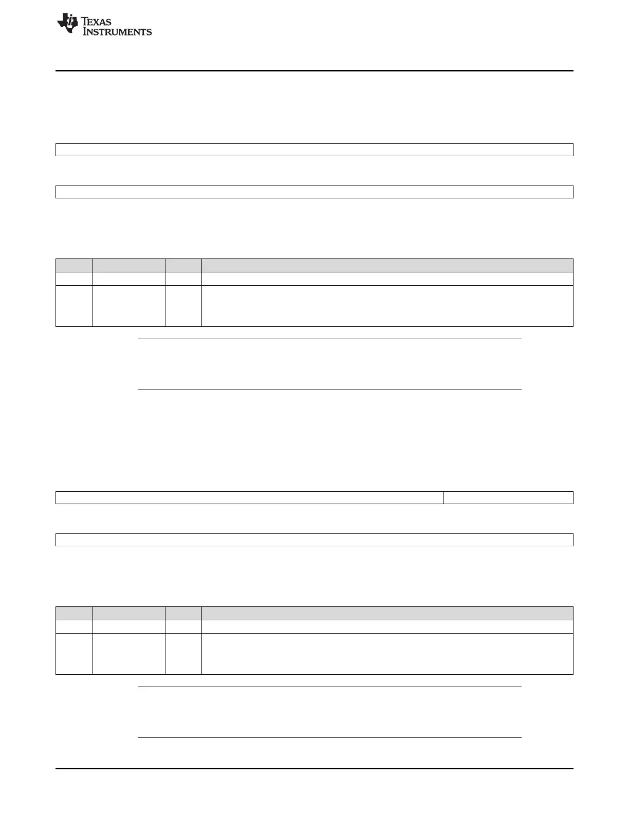
Figure 15-14 and Table 15-9 describe the DCC Valid0 Value register.
Figure 15-14. DCC Valid0 Value Register (DCCVALID0) [offset = 1Ch]
31 16
Reserved
R-0
15 0
VALID0
R-0
LEGEND: R = Read only; -n = value after reset
Table 15-9. DCC Valid0 Value Register (DCCVALID0) Field Descriptions
Bit Field Value Description
31-16 Reserved 0 Reads return 0. Writes have no effect.
15-0 VALID0 Current value for DCC Valid0.
Reads in any operating mode return the current value of Valid0.
Writes have no effect.
NOTE: Reads may not return exact current value of Valid0
Reading the Valid0 value while counting is enabled may not return the exact value of the
Valid0.
15.4.9 DCC Counter1 Value Register (DCCCNT1)
Figure 15-15 and Table 15-10 describe the DCC Counter1 Value register.
Figure 15-15. DCC Counter1 Value Register (DCCCNT1) [offset = 20h]
31 20 19 16
Reserved COUNT1
R-0 R/WP-0
15 0
COUNT1
R/WP-0
LEGEND: R/W = Read/Write; R = Read only; WP = Write in privileged mode only; -n = value after reset
Table 15-10. DCC Counter1 Value Register (DCCCNT1) Field Descriptions
Bit Field Value Description
31-20 Reserved 0 Reads return 0. Writes have no effect.
19-0 COUNT1 Current value for DCC counter1.
Reads in any operating mode return the current value of counter1.
Writes have no effect.
NOTE: Reads may not return exact current value of counter
Reading the counter1 value while counting is enabled may not return the exact value of the
counter1.
 Loading...