÷NR
÷R
PLL
÷1 - ÷64
÷1 - ÷256
÷1 - ÷32
INTCLK
Output CLK
PLL CLK
÷OD
÷1 - ÷8
post-ODCLK
CLKIN
÷NF
f
PLLCLK
f
CLKIN
NR
-----------------
x NF x x
1
OD
---------
1
R
----
=
www.ti.com
PLL
525
SPNU563A–March 2018
Submit Documentation Feedback
Copyright © 2018, Texas Instruments Incorporated
Oscillator and PLL
14.5 PLL
The following bit fields from PLLCTL1 and PLLCTL2 configure the PLL:
• REFCLKDIV[5:0]
• PLLMUL[15:0]
• ODPLL[2:0]
• PLLDIV[4:0]
• SPR_AMOUNT[8:0]
• SPREADINGRATE[8:0]
• FMENA
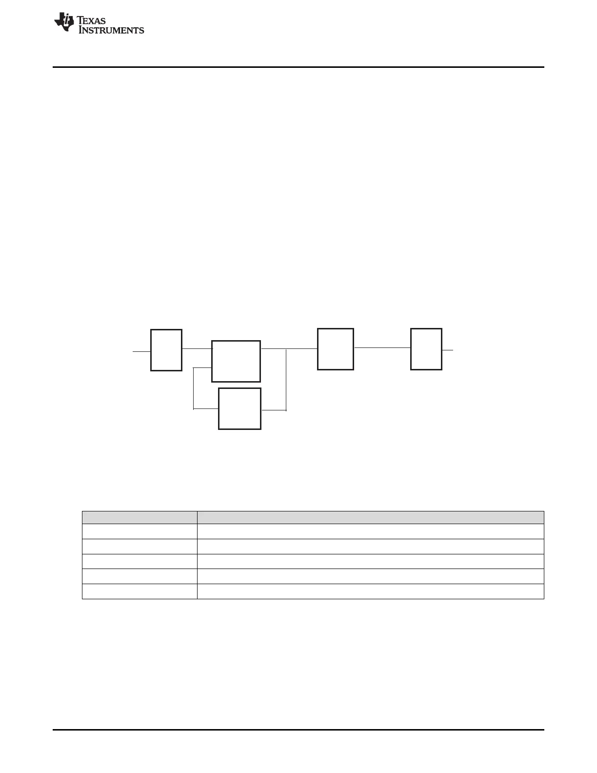
The PLL is responsible for synthesizing an output frequency from the input clock (from the oscillator);
Figure 14-4 shows a simple block diagram of the PLL. The FM-PLL divides the reference input for a lower
frequency input into the PLL (f
INTCLK
= f
CLKIN
/NR). The PLL multiplies this internal frequency by NF to get the
VCO output clock frequency (f
Output CLK
= f
INTCLK
× NF). The PLL output is subsequently divided by two
prescale values (OD and R). The value of OD is an integer from 1-8 and R is an integer from 1 to 32. This
output clock, PLL CLK, sources GCM clock source 1. Valid frequencies are shown in Table 14-1 while
Table 14-2 shows how that encoding is generated from the PLL bit fields.
[f
(post_ODCLK)
and f
(GCLK)
are data sheet parameters.]
Figure 14-4. Operation of the FM-PLL Module
Table 14-1. Valid Frequency Ranges for PLL
Frequency Limit
f
CLKIN
f
(OSC_Sqr)
f
INTCLK
1MHz - f
(OSC_Sqr)
f
Output CLK
150MHz - 550MHz
f
post-ODCLK
f
(post_ODCLK)
f
PLL CLK
f
(GCLK)
 Loading...


